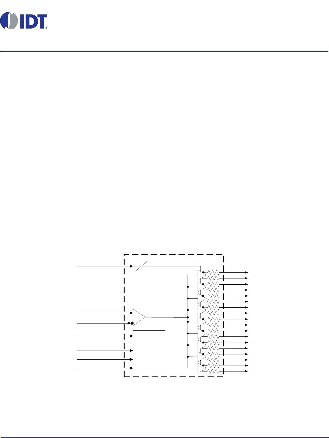
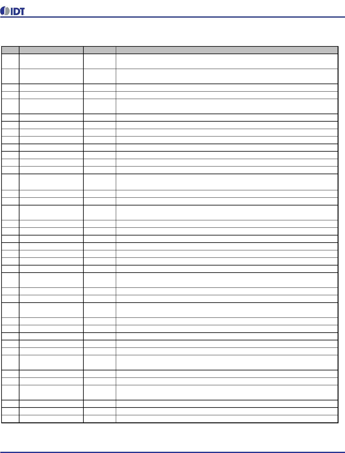
PIN # PIN NAME TYPE DESCRIPTION
1 vSADR_tri
LATCHED
IN
Tri-level latch to select SMBus Address. It has an internal 120kohm pull down
resistor. See SMBus Address Selection Table.
2vOE8# IN
Active low input for enabling output 8. This pin has an internal 120kohm pull-down.
1 = disable outputs, 0 = enable outputs.
3 DIF8 OUT Differential true clock output.
4 DIF8# OUT Differential complementary clock output.
5 VDDR1.5 PWR
1.5V power for differential input clock (receiver). This VDD should be treated as an
Analog power rail and filtered appropriately.
6 CLK_IN IN True input for differential reference clock.
7 CLK_IN# IN Complementary input for differential reference clock.
8 GNDR GND Analog ground pin for the differential input (receiver)
9 GNDDIG GND Ground pin for digital circuitry.
10 SCLK_3.3 IN Clock pin of SMBus circuitry, 3.3V tolerant.
11 SDATA_3.3 I/O Data pin for SMBus circuitry, 3.3V tolerant.
12 VDDDIG1.5 PWR 1.5V digital power (dirty power)
13 VDDIO PWR Power supply for differential outputs
14 vOE0# IN
Active low input for enabling output 0. This pin has an internal 120kohm pull-down.
1 = disable outputs, 0 = enable outputs.
15 DIF0 OUT Differential true clock output.
16 DIF0# OUT Differential complementary clock output.
17 vOE1# IN
Active low input for enabling output 1. This pin has an internal 120kohm pull-down.
1 = disable outputs, 0 = enable outputs.
18 DIF1 OUT Differential true clock output.
19 DIF1# OUT Differential complementary clock output.
20 VDD1.5 PWR Power supply, nominally 1.5V
21 VDDIO PWR Power supply for differential outputs
22 GND GND Ground pin.
23 DIF2 OUT Differential true clock output.
24 DIF2# OUT Differential complementary clock output.
25 vOE2# IN
Active low input for enabling output 2. This pin has an internal 120kohm pull-down.
1 = disable outputs, 0 = enable outputs.
26 DIF3 OUT Differential true clock output.
27 DIF3# OUT Differential complementary clock output.
28 vOE3# IN
Active low input for enabling output 3. This pin has an internal 120kohm pull-down.
1 = disable outputs, 0 = enable outputs.
29 GND GND Ground pin.
30 VDDO1.5 PWR Power supply for outputs, nominally 1.5V.
31 VDDIO PWR Power supply for differential outputs
32 DIF4 OUT Differential true clock output.
33 DIF4# OUT Differential complementary clock output.
34 vOE4# IN
Active low input for enabling output 4. This pin has an internal 120kohm pull-down.
1 = disable outputs, 0 = enable outputs.
35 DIF5 OUT Differential true clock output.
36 DIF5# OUT Differential complementary clock output.
37 vOE5# IN
Active low input for enabling output 5. This pin has an internal 120kohm pull-down.
1 = disable outputs, 0 = enable outputs.
38 VDD1.5 PWR Power supply, nominally 1.5V
39 VDDIO PWR Power supply for differential outputs
40 GND GND Ground pin.