DATASHEET
TWO OUTPUT DIFFERENTIAL BUFFER FOR PCIE GEN3
9DB233
IDT®
TWO OUTPUT DIFFERENTIAL BUFFER FOR PCIE GEN3 1
9DB233 OCTOBER 20, 2016
Description
The 9DB233 zero-delay buffer supports PCIe Gen3
requirements, while being backwards compatible to PCIe
Gen2 and Gen1. The 9DB233 is driven by a differential
SRC output pair from an IDT 932S421 or 932SQ420 or
equivalent main clock generator. It attenuates jitter on the
input clock and has a selectable PLL bandwidth to
maximize performance in systems with or without
Spread-Spectrum clocking. An SMBus interface allows
control of the PLL bandwidth and bypass options, while 2
clock request (OE#) pins make the 9DB233 suitable for
Express Card applications.
Recommended Application
2 output PCIe Gen3 zero-delay/fanout buffer
Output Features
2 - 0.7V current mode differential HCSL output pairs
Features/Benefits
OE# pins; suitable for Express Card applications
PLL or bypass mode; PLL can dejitter incoming clock
Selectable PLL bandwidth; minimizes jitter peaking in
downstream PLL's
Spread Spectrum Compatible; tracks spreading input
clock for low EMI
SMBus Interface; allows control of PLL BW and Mode
Key Specifications
Cycle-to-cycle jitter < 50 ps
Output-to-output skew < 50 ps
PCIe Gen3 phase jitter < 1.0ps RMS
Block Diagram
SPREAD
COMPATIBLE
PLL
CONTROL
LOGIC
SMBDAT
SMBCLK
SRC_IN
SRC_IN#
PLL_BW
IREF
DIF_0
DIF_1
OE1#
OE0#
9DB233
TWO OUTPUT DIFFERENTIAL BUFFER FOR PCIE GEN3
IDT®
TWO OUTPUT DIFFERENTIAL BUFFER FOR PCIE GEN3 2
9DB233 OCTOBER 20, 2016
Pin Configuration
Power Distribution Table
PLL_BW 1 20 VDDA
SRC_IN 2 19 GNDA
SRC_IN# 3 18 IREF
vOE0# 4 17 vOE1#
VDD 5 16 VDD
GND 6 15 GND
DIF_0 7 14 DIF_1
DIF_0# 8 13 DIF_1#
VDD 9 12 VDD
SMBDAT 10 11 SMBCLK
9DB233
Note:
Pins preceeded by ' v ' have internal
120K ohm pull down resistors
VDD GND
5,9,12,16 6,15 Differential Outputs
96 SMBUS
20 19 IREF
20 19 Analog VDD & GND for PLL core
Description
Pin Number
9DB233
TWO OUTPUT DIFFERENTIAL BUFFER FOR PCIE GEN3
IDT®
TWO OUTPUT DIFFERENTIAL BUFFER FOR PCIE GEN3 3
9DB233 OCTOBER 20, 2016
Pin Descriptions
PIN #
PIN
NAME
PIN TYPE DESCRIPTION
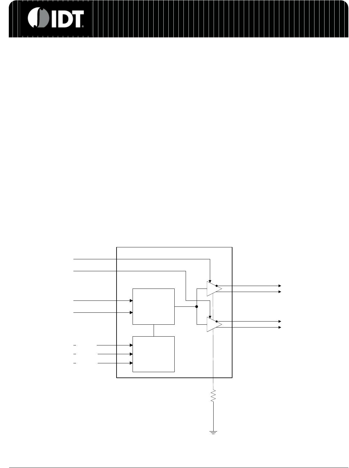
1 PLL_BW IN
3.3V input for selecting PLL Band Width
0 = low, 1= high
2 SRC_IN IN 0.7 V Differential SRC TRUE input
3 SRC_IN# IN 0.7 V Differential SRC COMPLEMENTARY input
4 vOE0# IN
Active low input for enabling DIF pair 0. This pin has an internal pull-down.
1 =disable outputs, 0 = enable outputs
5 VDD PWR Power supply, nominal 3.3V
6 GND PWR Ground pin.
7 DIF_0 OUT 0.7V differential true clock output
8 DIF_0# OUT 0.7V differential Complementary clock output
9 VDD PWR Power supply, nominal 3.3V
10 SMBDAT I/O Data pin of SMBUS circuitry, 5V tolerant
11 SMBCLK IN Clock pin of SMBUS circuitry, 5V tolerant
12 VDD PWR Power supply, nominal 3.3V
13 DIF_1# OUT 0.7V differential Complementary clock output
14 DIF_1 OUT 0.7V differential true clock output
15 GND PWR Ground pin.
16 VDD PWR Power supply, nominal 3.3V
17 vOE1# IN
Active low input for enabling DIF pair 1. This pin has an internal pull-down.
1 =disable outputs, 0 = enable outputs
18 IREF OUT
This pin establishes the reference for the differential current-mode output
pairs. It requires a fixed precision resistor to ground. 475ohm is the standard
value for 100ohm differential impedance. Other impedances require
different values. See data sheet.
19 GNDA PWR Ground pin for the PLL core.
20 VDDA PWR 3.3V power for the PLL core.
Pins preceeded by ' v ' have internal 120K ohm pull down resistors
Note:

9DB233AGILFT

Mfr. #:
Manufacturer:
IDT
Description:
Clock Buffer 2-output 3.3 V PCIe Gen1-2-3 Zero Delay / Fanout Buffer
Lifecycle:
New from this manufacturer.
Delivery:
DHL FedEx Ups TNT EMS
Payment:
T/T Paypal Visa MoneyGram Western Union