9DB233
TWO OUTPUT DIFFERENTIAL BUFFER FOR PCIE GEN3
IDT®
TWO OUTPUT DIFFERENTIAL BUFFER FOR PCIE GEN3 7
9DB233 OCTOBER 20, 2016
Electrical Characteristics–PCIe Phase Jitter Parameters
PARAMETER SYMBOL CONDITIONS MIN TYP MAX UNITS Notes
jp
hPCIeG1
(PLL BW of 2-4MHz, CDR = 10MHz)
(rms)
jp
hPCIeG1
10kHz < f < 1.5MHz
(rms)
Applies to all outputs.
See http://www.pcisi
g
.com for complete specs
Sample size of at least 100K cycles. This fi
g
ures extrapolates to 108ps pk-pk @ 1M cycles for a BER of 1-12.
9DB233
TWO OUTPUT DIFFERENTIAL BUFFER FOR PCIE GEN3
IDT®
TWO OUTPUT DIFFERENTIAL BUFFER FOR PCIE GEN3 8
9DB233 OCTOBER 20, 2016
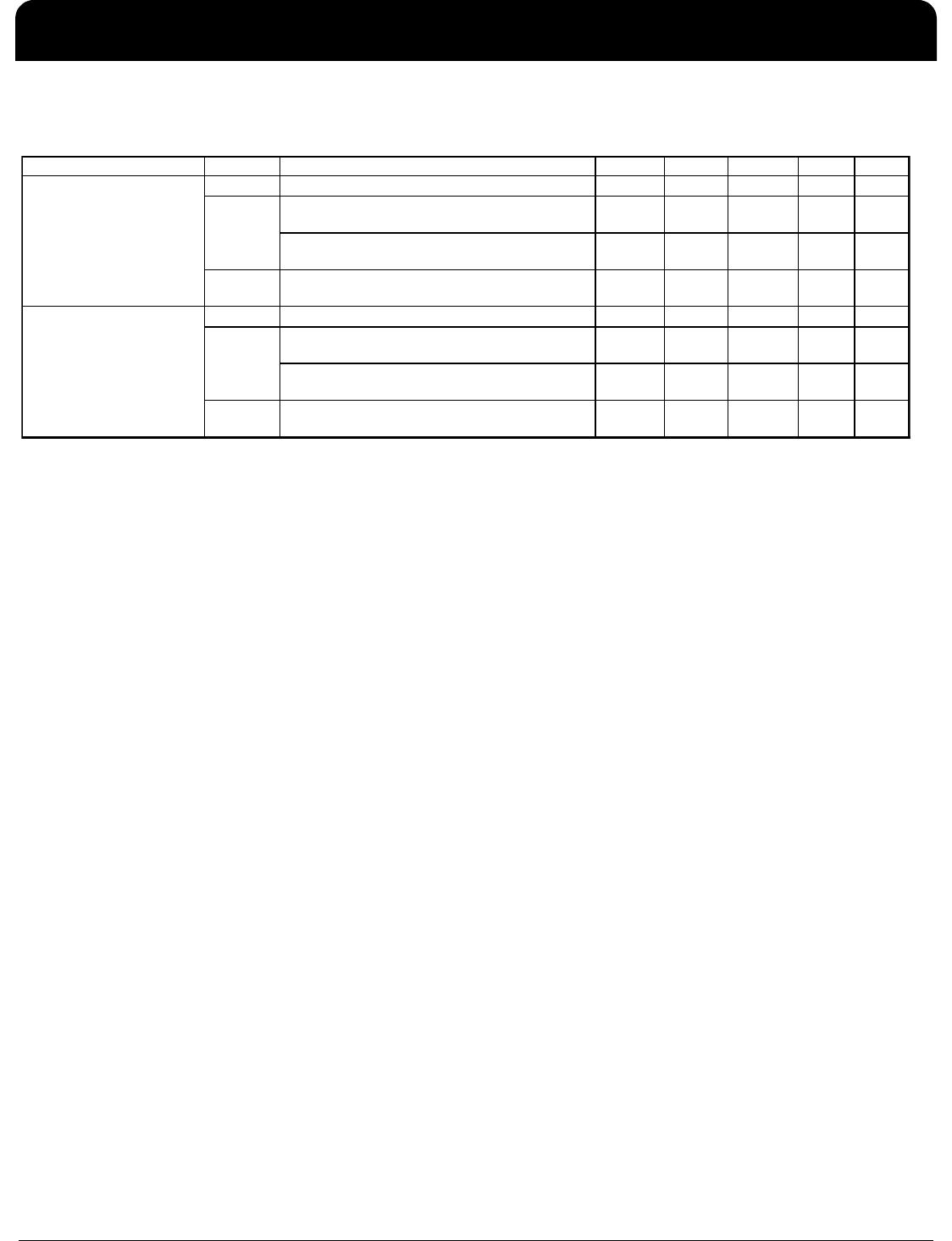
Common Recommendations for Differential Routing Dimension or Value Unit Figure
L1 length, route as non-coupled 50ohm trace 0.5 max inch 1
L2 length, route as non-coupled 50ohm trace 0.2 max inch 1
L3 length, route as non-coupled 50ohm trace 0.2 max inch 1
Rs 33 ohm 1
Rt 49.9 ohm 1
Down Device Differential Routing
L4 length, route as coupled microstrip 100ohm differential trace 2 min to 16 max inch 1
L4 length, route as coupled stripline 100ohm differential trace 1.8 min to 14.4 max inch 1
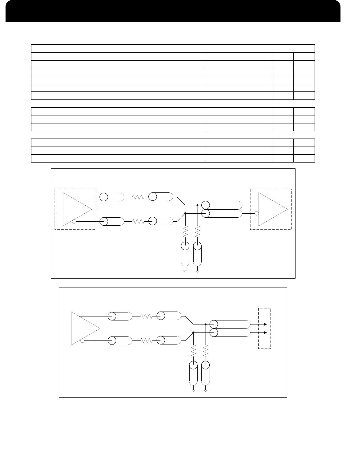
Differential Routing to PCI Express Connector
L4 length, route as coupled microstrip 100ohm differential trace 0.25 to 14 max inch 2
L4 length, route as coupled stripline 100ohm differential trace 0.225 min to 12.6 max inch 2
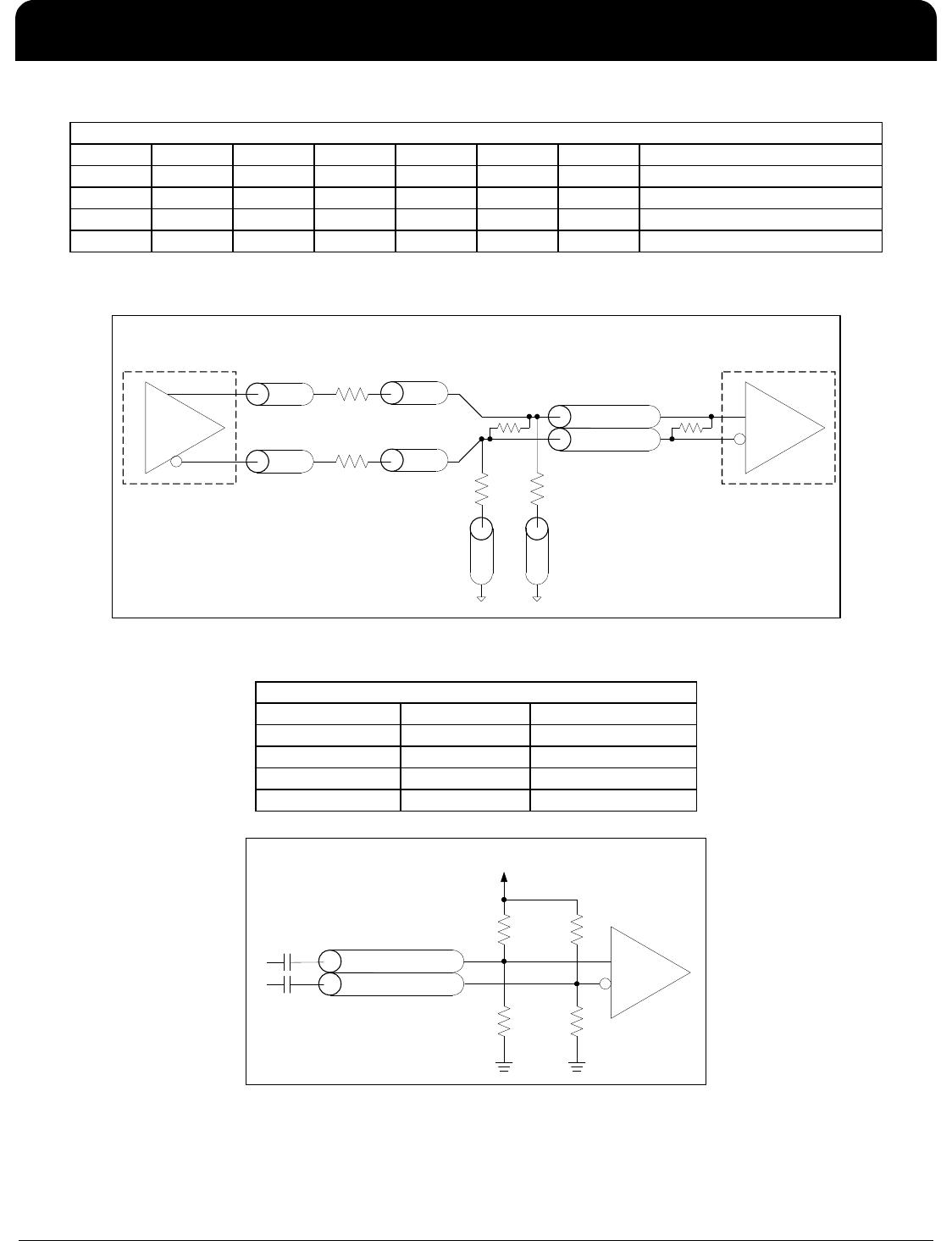
SRC Reference Clock
HCSL Output Buffer
L1
L1'
Rs
L2
L2'
Rs
L4'
L4
L3L3'
Rt Rt
PCI Express
Down Device
REF_CLK Input
Figure 1: Down Device Routing
HCSL Output Buffer
L1
L1'
Rs
L2
L2'
Rs
L4'
L4
L3L3'
Rt Rt
PCI Express
Add-in Board
REF_CLK Input
Figure 2: PCI Express Connector Routing
9DB233
TWO OUTPUT DIFFERENTIAL BUFFER FOR PCIE GEN3
IDT®
TWO OUTPUT DIFFERENTIAL BUFFER FOR PCIE GEN3 9
9DB233 OCTOBER 20, 2016
Vdiff Vp-p Vcm R1 R2 R3 R4 Note
0.45v 0.22v 1.08 33 150 100 100
0.58 0.28 0.6 33 78.7 137 100
0.80 0.40 0.6 33 78.7 none 100 ICS874003i-02 input compatible
0.60 0.3 1.2 33 174 140 100 Standard LVDS
R1a = R1b = R1
R2a = R2b = R2
Alternative Termination for LVDS and other Common Differential Signals (figure 3)
HCSL Output Buffer
L1
L1'
R1b
L2
L2'
R1a
L4'
L4
L3
R2a R2b
Down Device
REF_CLK Input
Figure 3
L3'
R3 R4
Component Value Note
R5a, R5b 8.2K 5%
R6a, R6b 1K 5%
Cc 0.1 µF
Vcm 0.350 volts
Cable Connected AC Coupled Application (figure 4)
PCIe Device
REF_CLK Input
Figure 4
R5a
L4'
L4
3.3 Volts
R5b
R6a R6b
Cc
Cc

9DB233AGILFT

Mfr. #:
Manufacturer:
IDT
Description:
Clock Buffer 2-output 3.3 V PCIe Gen1-2-3 Zero Delay / Fanout Buffer
Lifecycle:
New from this manufacturer.
Delivery:
DHL FedEx Ups TNT EMS
Payment:
T/T Paypal Visa MoneyGram Western Union