LT1011/LT1011A
1
1011afe
For more information www.linear.com/LT1011
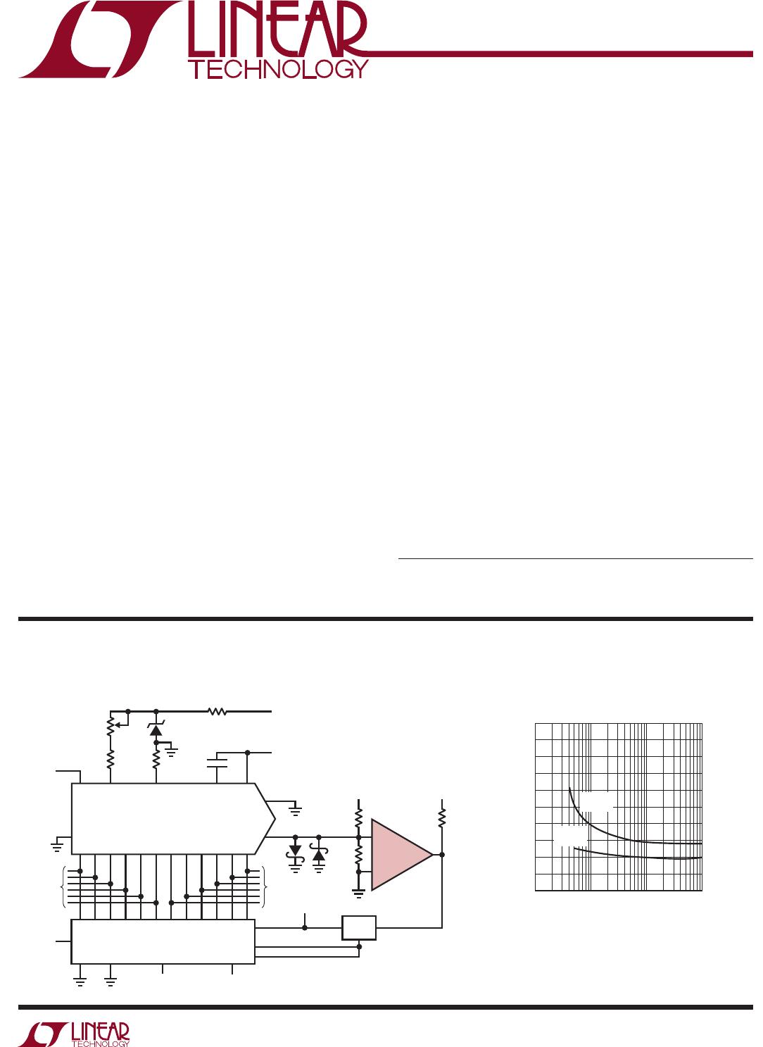
OVERDRIVE (mV)
0.1
200
RESPONSE TIME (ns)
250
300
350
400
1 10 100
1011 TA02
150
100
50
0
450
500
FALLING
OUTPUT
RISING
OUTPUT
10µs 12-Bit A/D Converter
Response Time vs Overdrive
Typical applicaTion
DescripTion
Voltage Comparator
The LT
®
1011 is a general purpose comparator with sig-
nificantly better input characteristics than the LM111.
Although pin compatible with the LM111, it offers four
times lower bias current, six times lower offset voltage
and five times higher voltage gain. Offset voltage drift,
a previously unspecified parameter, is guaranteed at
15µV/°C. Additionally, the supply current is lower by
a factor of two with no loss in speed. The LT1011 is
several times faster than the LM111 when subjected to
large overdrive conditions. It is also fully specified for DC
parameters and response time when operating on a single
5V supply. The LT1011 retains all the versatile features of
the LM111, including single 3V to ±18V supply operation,
and a floating transistor output with 50mA source/sink
capability. It can drive loads referenced to ground, nega-
tive supply or positive supply, and is specified up to 50V
between V
–
and the collector output. A differential input
voltage up to the full supply voltage is allowed, even with
±18V supplies, enabling the inputs to be clamped to the
supplies with simple diode clamps.
FeaTures
applicaTions
n
Pin Compatible with LM111 Series Devices
n
Guaranteed Max 0.5mV Input Offset Voltage
n
Guaranteed Max 25nA Input Bias Current
n
Guaranteed Max 3nA Input Offset Current
n
Guaranteed Max 250ns Response Time
n
Guaranteed Min 200,000 Voltage Gain
n
50mA Output Current Source or Sink
n
±30V Differential Input Voltage
n
Fully Specified for Single 5V Operation
n
Available in 8-Lead PDIP and SO Packages
n
SAR A/D Converters
n
Voltage-to-Frequency Converters
n
Precision RC Oscillator
n
Peak Detector
n
Motor Speed Control
n
Pulse Generator
n
Relay/Lamp Driver
6012
12-BIT
D/A CONVERTER
PARALLEL
OUTPUTS
PARALLEL
OUTPUTS
*R2 AND R4
SHOULD TC TRACK
R6
820Ω
R3
6.98k
R2*
6.49k
R1
1k
FULL-SCALE
TRIM
LM329
7V
R4*
2.49k
R5
1k
0.001µF
–15V
15V
15V
5V
SERIAL OUTPUT
INPUT
0V TO 10V 5V
7475
LATCH
AM2504
SAR REGISTER
START CLOCK f = 1.4MHz
1011 TA01
S CP
D
CC
S
E
–
+
LT1011A
L, LT , LTC , LT M, Linear Technology and the Linear logo are registered trademarks of Linear
Technology Corporation. All other trademarks are the property of their respective owners.