LT1011/LT1011A
4
1011afe
For more information www.linear.com/LT1011
elecTrical characTerisTics
Note 1: Stresses beyond those listed under Absolute Maximum Ratings
may cause permanent damage to the device. Exposure to any Absolute
Maximum Rating condition for extended periods may affect device
reliability and lifetime.
Note 2: Inputs may be clamped to supplies with diodes so that
maximum input voltage actually exceeds supply voltage by one diode
drop. See Input Protection in the Applications Information section.
Note 3: T
JMAX
= 150°C.
Note 4: Output is sinking 1.5mA with V
OUT
= 0V.
Note 5: These specifications apply for all supply voltages from a single
5V to ±15V, the entire input voltage range, and for both high and low
output states. The high state is I
SINK
= 100µA, V
OUT
= (V
+
– 1V) and
the low state is I
SINK
= 8mA, V
OUT
= 0.8V. Therefore, this specification
The l denotes the specifications which apply over the full operating
temperature range, otherwise specifications are at T
A
= 25°C. V
S
= ±15V, V
CM
= 0V, R
S
= 0Ω, V
GND
= –15V, output at pin 7 unless
otherwise noted.
SYMBOL PARAMETER CONDITIONS
LT1011AC/AI/AM LT1011C/I/M
UNITSMIN TYP MAX MIN TYP MAX
V
OS
Input Offset Voltage (Note 4)
0.3 0.5
1
0.6 1.5
3
mV
mV
*Input Offset Voltage R
S
≤ 50k (Note 5)
0.75
1.5
2
3
mV
mV
I
OS
*Input Offset Current (Note 5)
0.2 3
5
0.2 4
6
nA
nA
I
B
Input Bias Current (Note 4) 15 25 20 50 nA
*Input Bias Current (Note 5)
20 35
50
25 65
80
nA
nA
∆V
OS
T
Input Offset Voltage Drift
(Note 6)
T
MIN
≤ T ≤ T
MAX
4 15 4 25 µV/°C
A
VOL
*Large-Signal Voltage Gain R
L
= 1k Connected to 15V,
–10V ≤ V
OUT
≤ 14.5V
200 500 200 500 V/mV
R
L
= 500Ω Connected to 5V,
V
S
= Single 5V, V
GND
= 0V,
0.5V ≤ V
OUT
≤ 4.5V
50 300 50 300 V/mV
CMRR Common Mode Rejection Ratio 94 115 90 115 dB
*Input Voltage Range (Note 9) V
S
= ±15V
V
S
= Single 5V
14.5
0.5
13
3
14.5
0.5
13
3
V
V
t
D
*Response Time (Note 7) 150 250 150 250 ns
V
OL
*Output Saturation Voltage,
V
GND
= 0
V
IN
= –5mV, I
SINK
= 8mA, T
J
≤ 100°C
V
IN
= –5mV, I
SINK
= 8mA
V
IN
= –5mV, I
SINK
= 50mA
0.25
0.25
0.7
0.4
0.45
1.5
0.25
0.25
0.7
0.4
0.45
1.5
V
V
V
*Output Leakage Current V
IN
= 5mV, V
GND
= –15V,
V
OUT
= 20V
0.2 10
500
0.2 10
500
nA
nA
*Positive Supply Current V
GND
= 0 3.2 4 3.2 4 mA
*Negative Supply Current V
GND
= 0 1.7 2.5 1.7 2.5 mA
*Strobe Current (Note 8) Minimum to Ensure Output Transistor is Off,
V
GND
= 0
500 500 µA
Input Capacitance 6 6 pF
*Indicates parameters which are guaranteed for all supply voltages, including a single 5V supply. See Note 5.
defines a worst-case error band that includes effects due to common
mode signals, voltage gain and output load.
Note 6: Drift is calculated by dividing the offset voltage difference
measured at min and max temperatures by the temperature difference.
Note 7: Response time is measured with a 100mV step and 5mV
overdrive. The output load is a 500Ω resistor tied to 5V. Time
measurement is taken when the output crosses 1.4V.
Note 8: Do not short the STROBE pin to ground. It should be current
driven at 3mA to 5mA for the shortest strobe time. Currents as low
as 500µA will strobe the LT1011A if speed is not important. External
leakage on the STROBE pin in excess of 0.2µA when the strobe is “off”
can cause offset voltage shifts.
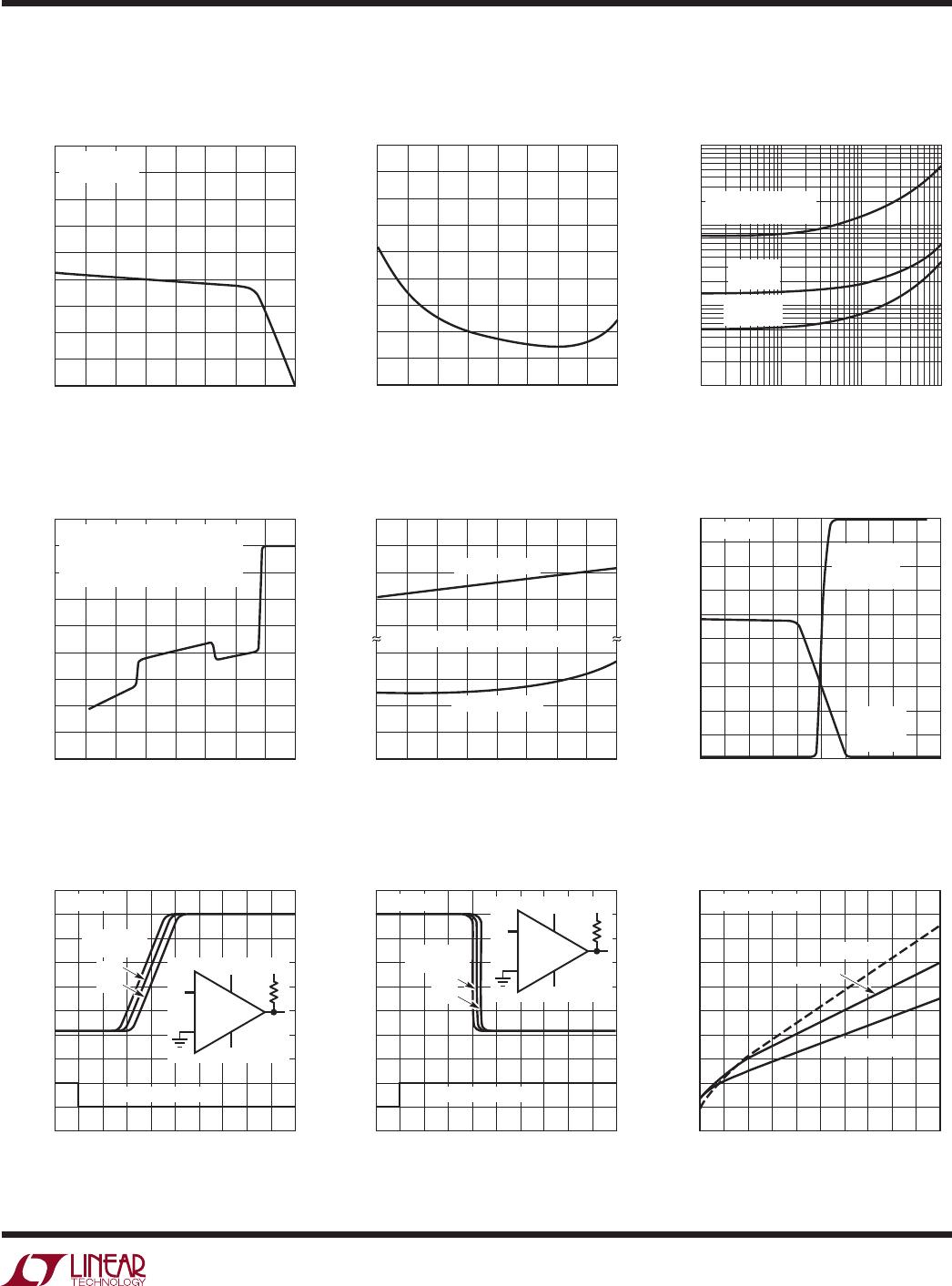
Note 9: See graph “Input Offset Voltage vs Common Mode Voltage.”
LT1011/LT1011A
5
1011afe
For more information www.linear.com/LT1011
TEMPERATURE (°C)
–50
CURRENT (nA)
25
30
35
50 75 100 125
150
1011 G01
20
15
0
–25
0
25
5
10
45
40
I
B
FLOWS OUT
OF INPUTS
TEMPERATURE (°C)
–50
CURRENT (nA)
0.5
0.6
0.7
50 75 100 125
150
1011 G02
0.4
0.3
0
–25
0
25
0.1
0.2
0.9
0.8
SOURCE RESISTANCE (Ω)
1k
0.1
EQUIVALENT OFFSET VOLTAGE (mV)
1
10
100
10k 100k 1M
1011 G03
LM311
(FOR COMPARISON)
LT1011M
LT1011C
LT1011AM
LT1011AC
Typical perForMance characTerisTics
Input Characteristics* Common Mode Limits Transfer Function (Gain)
Response Time—Collector Output Response Time—Collector Output
Collector Output Saturation
Voltage
Input Bias Current Input Offset Current Worst-Case Offset Error
INPUT VOLTAGE (V)
–20
INPUT CURRENT (nA)
–15
–10
–5
0 5 10 15
20
1011 G04
–20
–25
–40
–15
–10
–5
–35
–30
5
0
*EITHER INPUT.
REMAINING INPUT GROUNDED.
CURRENT FLOWS OUT OF INPUT.
V
S
= ±15V
TEMPERATURE (°C)
–50
COMMON MODE VOLTAGE (V)
–2.0
–1.5
–1.0
50 75 100 125
150
1011 G05
0.4
0.3
V
–25
0
25
0.1
0.2
V
+
–0.5
REFERRED TO SUPPLIES
POSITIVE LIMIT
NEGATIVE LIMIT
DIFFERENTIAL INPUT VOLTAGE (mV)
– 0.5
30
40
50
0.3
1011 G06
20
OUTPUT VOLTAGE (V)
10
0
–0.3
–0.1
0.1
0.5
T
A
= 25°C
COLLECTOR
OUTPUT
R
L
= 1k
EMITTER
OUTPUT
R
L
= 600Ω
TIME (ns)
0
2
4
350
1011 G07
0
100mV
1
3
5
0
50 100
150
250 300 400
200
450
V
S
= ±15V
5mV
2mV
OVERDRIVE
20mV
INPUT = 100mV STEP
15V 5V
500Ω
V
IN
–15V
+
TIME (ns)
0
2
4
6
350
1011 G08
0
0
1
3
5
–100mV
50 100
150
250 300 400
200
450
V
S
= ±15V
5mV
2mV
OVERDRIVE
20mV
INPUT = 100mV STEP
15V 5V
500Ω
V
IN
–15V
+
SINK CURRENT (mA)
SATURATION VOLTAGE (V)
50
0.6
0.8
1.0
40
1011 G09
0.4
0.3
0.2
0.5
0.7
0.9
0.1
0
10 15
20
30 35 45
25
50
PIN 1 GROUNDED
T
A
= 125°C
T
A
= –55°C
T
A
= 25°C
LT1011/LT1011A
6
1011afe
For more information www.linear.com/LT1011
Typical perForMance characTerisTics
Supply Current vs Supply Voltage Supply Current vs Temperature Output Leakage Current
Output Saturation—
Ground Output Output Saturation Voltage Response Time vs Input Step Size
Response Time Using GND Pin
as Output
Response Time Using GND Pin
as Output Output Limiting Characteristics*
TIME (µs)
0
INPUT VOLTAGE (mV)
OUTPUT VOLTAGE (V)
0
10
15
2
4
1011 G10
–100
0
–10
–50
5
–5
–15
1
3
20mV 5mV 2mV
V
S
= ±15V
T
A
= 25°C
2k
V
OUT
V
IN
V
V
+
+
TIME (µs)
0
INPUT VOLTAGE (mV) OUTPUT VOLTAGE (V)
–100
10
15
2
4
1011 G11
0
0
–10
–50
5
–5
–15
1
3
20mV
V
S
= ±15V
T
A
= 25°C
5mV 2mV
2k
V
OUT
V
IN
V
V
+
+
OUTPUT VOLTAGE (V)
0
0
20
40
60
80
100
120
140
0
0.1
0.2
0.3
0.4
0.5
0.6
0.7
1011 G12
5
10 15
SHORT-CIRCUIT CURRENT (mA)
POWER DISSIPATION (W)
SHORT-CIRCUIT
CURRENT
*MEASURED 3 MINUTES
AFTER SHORT
POWER
DISSIPATION
T
A
= 25°C
SUPPLY VOLTAGE (V)
0
0
CURRENT (mA)
1
2
3
4
5
5
10 15 20
1011 G13
25 30
POSITIVE SUPPLY
COLLECTOR OUTPUT “LO”
POSITIVE AND NEGATIVE SUPPLY
COLLECTOR OUTPUT “HI”
TEMPERATURE (˚C)
–50
CURRENT (mA)
4
5
6
25 75
1011 G14
3
2
–25 0
50 100 125
1
0
POSITIVE SUPPLY
COLLECTOR OUTPUT “LO”
POSITIVE AND NEGATIVE SUPPLY
COLLECTOR OUTPUT “HI”
TEMPERATURE (°C)
10
–10
LEAKAGE CURRENT (A)
10
–9
10
–8
10
–7
25 65 85 105
10
–11
45 125
1011 G15
V
S
= ±15V
V
OUT
= 35V
V
GND
= –15V
OUTPUT CURRENT (mA)
0
V
+
TO GROUND PIN VOLTAGE (V)
3
4
5
40
1011 G16
2
1
0
10
20
30
50
T
J
= 125°C
T
J
= 25°C
T
J
= –55°C
REFERRED TO V
+
2
3
4
1
7
8
V
+
V
R
L
V
OUT
+
+
LT1011
INPUT OVERDRIVE (mV)
0
0
SATURATION VOLTAGE (V)
0.1
0.2
0.3
0.4
2 4
6
8
1011 G17
0.5
0.6
1 3
5
7
I
SINK
= 8mA
T
J
= 125°C
T
J
= 25°C
T
J
= –55°C
INPUT STEP (V)
0
PROPAGATION DELAY (ns)
600
800
1000
8
1011 G18
400
200
0
2
4
6
1 9
3
5
7
10
V
S
= ±15V
R
L
= 500Ω TO 5V
OVERDRIVE = 5mV
+
3
INPUT
500Ω
2
1
7
5V
RISING INPUT
FALLING INPUT

LT1011CN8#PBF

Mfr. #:
Manufacturer:
Analog Devices Inc.
Description:
Analog Comparators Prec Volt COMPARATOR
Lifecycle:
New from this manufacturer.
Delivery:
DHL FedEx Ups TNT EMS
Payment:
T/T Paypal Visa MoneyGram Western Union