LT1011/LT1011A
10
1011afe
For more information www.linear.com/LT1011
applicaTions inForMaTion
The input resistors should limit fault current to a reasonable
value (0.1mA to 20mA). Power dissipation in the resis-
tors must be considered for continuous faults, especially
when the LT1011 supplies are off. One final caution: lightly
loaded supplies may be forced to higher voltages by large
fault currents flowing through D1-D4.
R3 and R4 limit input current to the LT1011 to less than
1mA when the input signals are held below V
–
. They may
be eliminated if R1 and R2 are large enough to limit fault
current to less than 1mA.
Input Slew Rate Limitations
The response time of a comparator is typically measured
with a 100mV step and a 5mV to 10mV overdrive. Unfor-
tunately, this does not simulate many real world situations
where the step size is typically much larger and overdrive
can be significantly less. In the case of the LT1011, step
size is important because the slew rate of internal nodes
will limit response time for input step sizes larger than
1V. At 5V step size, for instance, response time increases
from 150ns to 360ns. See the curve “Response Time vs
Input Step Size for more detail.
If
response time
is critical and large input signals are ex-
pected, clamp diodes across the inputs are recommended.
The slew rate limitation can also affect performance when
differential input voltage is low, but both inputs must
slew quickly. Maximum suggested common mode slew
rate is 10V/µs.
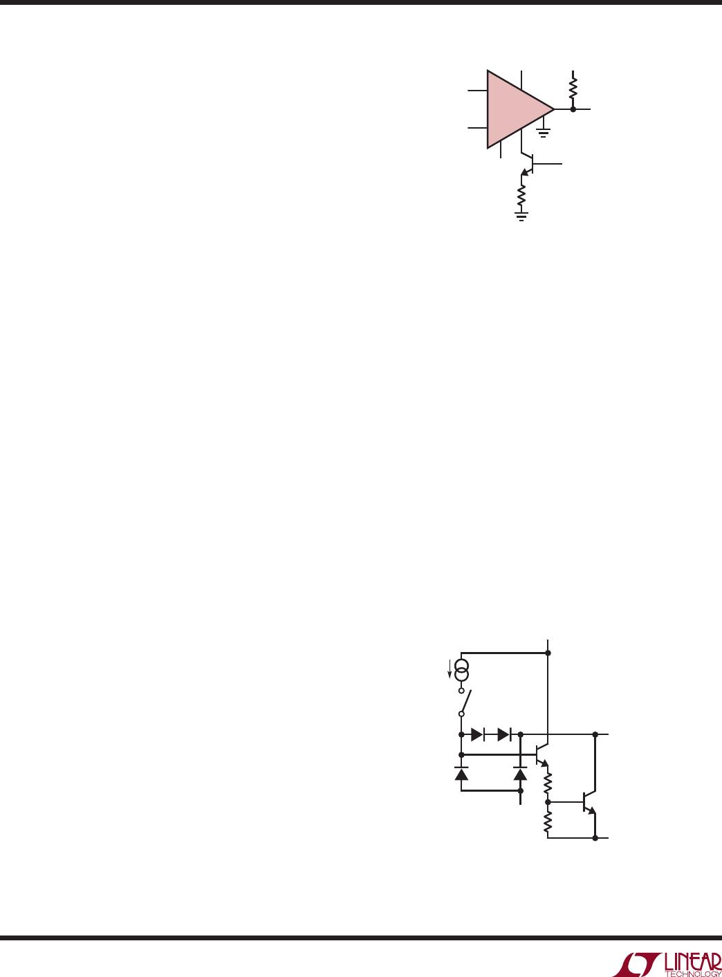
Strobing
The LT1011 can be strobed by pulling current out of the
STROBE pin. The output transistor is forced to an “off”
state, giving a “hi” output at the collector (Pin 7). Currents
as low as 250µA will cause strobing, but at low strobe
currents, strobe delay will be 200ns to 300ns. If strobe
current is increased to 3mA, strobe delay drops to about
60ns. The voltage at the STROBE pin is about 150mV below
V
+
at zero strobe current and about 2V below V
+
for 3mA
strobe current. Do not ground the STROBE pin. It must
be current driven. Figure 4 shows a typical strobe circuit.
Note that there is no bypass capacitor between Pins 5 and
6. This maximizes strobe speed, but leaves the compara-
tor more sensitive to oscillation problems for slow, low
Figure 4. Typical Strobe Circuit
Figure 5. Output Transistor Circuitry
level inputs. A 1pF capacitor between the output and Pin
5 will greatly reduce
oscillation problems without reduc-
ing strobe speed.
DC hysteresis can also be added by placing a resistor
from the output to Pin 5. See step 5 under “Preventing
Oscillation Problems.”
The pin (6) used for strobing is also one of the offset adjust
pins. Current flow into or out of Pin 6 must be kept very
low (<0.2µA) when not strobing to prevent input offset
voltage shifts.
Output Transistor
The LT1011 output transistor is truly floating in the sense
that no current flows into or out of either the collector
or emitter when the transistor is in the “off” state. The
equivalent circuit is shown in Figure 5.
–
+
LT1011
R
L
3k
TTL OR
CMOS DRIVE
(5V SUPPLY)
OUTPUT
–15
8
6
1
7
4
1011 F04
3
2
R1
170Ω
R2
470Ω
Q1
V
+
D2
I
1
0.5mA
1011 F05
V
–
D1
Q2
EMITTER
(GND PIN)
COLLECTOR
(OUTPUT)
OUTPUT
TRANSISTOR