AD811 Data Sheet
APPLICATIONS INFORMATION
GENERAL DESIGN CONSIDERATIONS
The AD811 is a current feedback amplifier optimized for use in
high performance video and data acquisition applications.
Because it uses a current feedback architecture, its closed-loop
−3 dB bandwidth is dependent on the magnitude of the
feedback resistor. The desired closed-loop gain and bandwidth
are obtained by varying the feedback resistor (R
FB
) to tune the
bandwidth and by varying the gain resistor (R
G
) to obtain the
correct gain. Table 3 contains recommended resistor values for
a variety of useful closed-loop gains and supply voltages.
Table 3. −3 dB Bandwidth vs. Closed-Loop Gain and
Resistance Values
V
S
= ±15 V
Closed-Loop Gain R
FB
R
G
−3 dB BW (MHz)
+1 750 Ω 140
+2 649 Ω 649 Ω 120
+10 511 Ω 56.2 Ω 100
1
590 Ω 590 Ω 115
−10 511 Ω 51.1 Ω 95
V
S
= ±5 V
Closed-Loop Gain R
FB
R
G
−3 dB BW (MHz)
+1 619 Ω 80
+2 562 Ω 562 Ω 80
+10 442 Ω 48.7 Ω 65
1
562 Ω 562 Ω 75
10
442 Ω 44.2 Ω 65
V
S
= ±10 V
Closed-Loop Gain R
FB
R
G
−3 dB BW (MHz)
+1 649 Ω 105
+2 590 Ω 590 Ω 105
+10 499 Ω 49.9 Ω 80
−1 590 Ω 590 Ω 105
−10 499 Ω 49.9 Ω 80
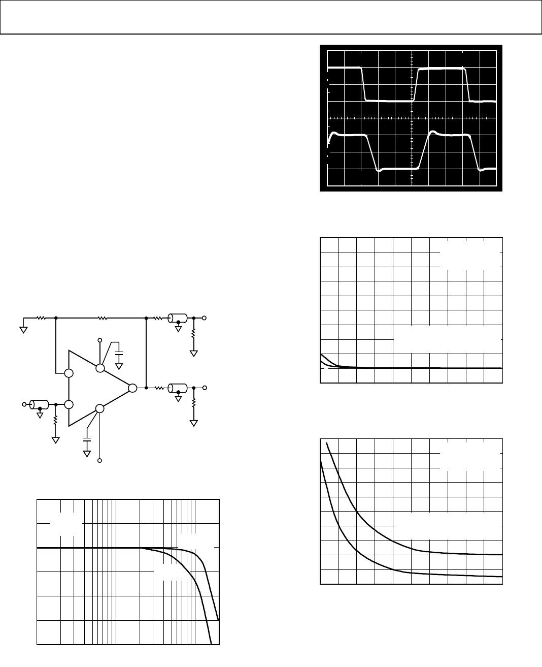
Figure 17 and Figure 18 illustrate the relationship between the
feedback resistor and the frequency and time domain response
characteristics for a closed-loop gain of +2. (The response at
other gains is similar.)
The 3 dB bandwidth is somewhat dependent on the power
supply voltage. As the supply voltage is decreased, for example,
the magnitude of the internal junction capacitances is increased,
causing a reduction in closed-loop bandwidth. To compensate
for this, smaller values of feedback resistor are used at lower
supply voltages.
ACHIEVING THE FLATTEST GAIN RESPONSE AT
HIGH FREQUENCY
Achieving and maintaining gain flatness of better than 0.1 dB at
frequencies above 10 MHz requires careful consideration of
several issues.
Choice of Feedback and Gain Resistors
Because of the previously mentioned relationship between the
3 dB bandwidth and the feedback resistor, the fine scale gain
flatness varies, to some extent, with feedback resistor tolerance.
Therefore, it is recommended that resistors with a 1% tolerance
be used if it is desired to maintain flatness over a wide range of
production lots. In addition, resistors of different construction
have different associated parasitic capacitance and inductance.
Metal film resistors were used for the bulk of the character-
ization for this data sheet. It is possible that values other than
those indicated are optimal for other resistor types.
Printed Circuit Board Layout Considerations
As is expected for a wideband amplifier, PC board parasitics can
affect the overall closed-loop performance. Of concern are stray
capacitances at the output and the inverting input nodes. If a
ground plane is used on the same side of the board as the signal
traces, a space (3/16" is plenty) should be left around the signal
lines to minimize coupling. Additionally, signal lines connecting
the feedback and gain resistors should be short enough so that
their associated inductance does not cause high frequency gain
errors. Line lengths less than 1/4" are recommended.
Quality of Coaxial Cable
Optimum flatness when driving a coax cable is possible only
when the driven cable is terminated at each end with a resistor
matching its characteristic impedance. If the coax is ideal, then
the resulting flatness is not affected by the length of the cable.
While outstanding results can be achieved using inexpensive
cables, note that some variation in flatness due to varying cable
lengths may occur.
Power Supply Bypassing
Adequate power supply bypassing can be critical when optimiz-
ing the performance of a high frequency circuit. Inductance in
the power supply leads can form resonant circuits that produce
peaking in the amplifier’s response. In addition, if large current
transients must be delivered to the load, then bypass capacitors
(typically greater than 1 µF) are required to provide the best
settling time and lowest distortion. Although the recommended
0.1 µF power supply bypass capacitors are sufficient in many
applications, more elaborate bypassing (such as using two
paralleled capacitors) may be required in some cases.
Rev. G | Page 12 of 20
Data Sheet AD811
Driving Capacitive Loads
The feedback and gain resistor values in Table 3 result in very
flat closed-loop responses in applications where the load
capacitances are below 10 pF. Capacitances greater than this
result in increased peaking and overshoot, although not
necessarily in a sustained oscillation.
There are at least two very effective ways to compensate for this
effect. One way is to increase the magnitude of the feedback
resistor, which lowers the 3 dB frequency. The other method is
to include a small resistor in series with the output of the ampli-
fier to isolate it from the load capacitance. The results of these
two techniques are illustrated in Figure 38. Using a 1.5 kΩ
feedback resistor, the output ripple is less than 0.5 dB when
driving 100 pF. The main disadvantage of this method is that it
sacrifices a little bit of gain flatness for increased capacitive load
drive capability. With the second method, using a series resistor,
the loss of flatness does not occur.
Figure 37. Recommended Connection for Driving a Large Capacitive Load
Figure 38. Performance Comparison of Two Methods
for Driving a Capacitive Load
Figure 39. Recommended Value of Series Resistor vs.
the Amount of Capacitive Load
Figure 39 shows recommended resistor values for different load
capacitances. Refer again to Figure 38 for an example of the
results of this method. Note that it may be necessary to adjust
the gain setting resistor, R
G
, to correct for the attenuation which
results due to the divider formed by the series resistor, R
S
, and
the load resistance.
Applications that require driving a large load capacitance at a
high slew rate are often limited by the output current available
from the driving amplifier. For example, an amplifier limited to
25 mA output current cannot drive a 500 pF load at a slew rate
greater than 50 V/µs. However, because of the 100 mA output
current of the AD811, a slew rate of 200 V/µs is achievable
when driving the same 500 pF capacitor, as shown in Figure 40.
Figure 40. Output Waveform of an AD811 Driving a 500 pF Load.
Gain = +2, R
FB
= 649 Ω, R
S
= 15 Ω, R
S
= 10 kΩ
AD811
+
7
6
4
2
3
R
S
(OPTIONAL)
C
L
R
L
V
OUT
–V
S
+V
S
R
FB
R
G
R
T
V
IN
0.1µF
0.1µF
00866-E-038
–6
–3
0
3
6
9
12
GAIN (dB)
FREQUENCY (MHz)
1 10 100
00866-E-039
V
S
= ±15V
C
L
= 100pF
R
L
= 10k
GAIN = +2
R
FB
= 1.5k
R
S
= 0
R
FB
= 649
R
S
= 30
0
10
20
30
40
50
60
70
80
90
100
VALUE OF R
S
()
LOAD CAPACITANCE (pF)
10 100 1000
00866-E-040
GAIN = +2
V
S
= ±15V
R
S
VALUE SPECIFIED
IS FOR FLATTEST
FREQUENCY RESPONSE
00866-E-041
10
90
100
0%
5V
2V
100ns
V
IN
V
OUT
Rev. G | Page 13 of 20
AD811 Data Sheet
OPERATION AS A VIDEO LINE DRIVER
The AD811 has been designed to offer outstanding performance
at closed-loop gains of +1 or greater, while driving multiple
reverse-terminated video loads. The lowest differential gain and
phase errors are obtained when using ±15 V power supplies.
With ±12 V supplies, there is an insignificant increase in these
errors and a slight improvement in gain flatness. Due to power
dissipation considerations, ±12 V supplies are recommended
for optimum video performance. Excellent performance can be
achieved at much lower supplies as well.
The closed-loop gain versus the frequency at different supply
voltages is shown in Figure 42. Figure 43 is an oscilloscope
photograph of an AD811 line drivers pulse response with
±15 V supplies. The differential gain and phase error versus the
supply are plotted in Figure 44 and Figure 45, respectively.
Another important consideration when driving multiple cables
is the high frequency isolation between the outputs of the
cables. Due to its low output impedance, the AD811 achieves
better than 40 dB of output-to-output isolation at 5 MHz
driving back-terminated 75 Ω cables.
Figure 41. A Video Line Driver Operating at a Gain of +2
Figure 42. Closed-Loop Gain vs. Frequency, Gain = +2
Figure 43. Small Signal Pulse Response, Gain = +2, V
S
= ±15 V
Figure 44. Differential Gain Error vs. Supply Voltage for
the Video Line Driver of Figure 41
Figure 45. Differential Phase Error vs. Supply Voltage for
the Video Line Driver of Figure 41
V
IN
–V
S
+V
S
0.1µF
0.1µF
AD811
V
OUT
No. 2
V
OUT
No. 1
75 CABLE
75 CABLE
75 CABLE
75
75
649649
75
75
75
+
7
6
4
3
2
00866-E-042
–6
–3
0
3
6
9
12
GAIN (dB)
FREQUENCY (MHz)
1 10 100
00866-E-043
V
S
= ±15V
R
FB
= 649
V
S
= ±5V
R
FB
= 562
G = +2
R
L
= 150
R
G
= R
FB
00866-E-044
10
90
100
0%
1
V
1
V
10n
s
V
IN
V
OUT
0
0.01
0.02
0.03
0.04
0.05
0.06
0.07
0.08
0.09
0.10
DIFFERENTIAL GAIN (%)
5 6 7 8 9 10 11 12
13 14 15
SUPPLY VOLTAGE (V)
00866-E-045
R
F
= 649
F
C
= 3.58MHz
100 IRE
MODULATED RAMP
a. DRIVING A SINGLE, BACK-
TERMINATED, 75 COAX CABLE
b. DRIVING TWO PARALLEL, BACK-
TERMINATED, COAX CABLES
a
b
0
0.02
0.04
0.06
0.08
0.10
0.12
0.14
0.16
0.18
0.20
DIFFERENTIAL PHASE (DEGREES)
5 6 7 8 9 10 11 12 13 14 15
SUPPLY VOLTAGE (V)
00866-E-046
R
F
= 649
F
C
= 3.58MHz
100 IRE
MODULATED RAMP
a. DRIVING A SINGLE, BACK-
TERMINATED, 75 COAX CABLE
b. DRIVING TWO PARALLEL, BACK-
TERMINATED, COAX CABLES
a
b
Rev. G | Page 14 of 20

AD811JRZ

Mfr. #:
Manufacturer:
Analog Devices Inc.
Description:
Video Amplifiers AD811 Eval Brd
Lifecycle:
New from this manufacturer.
Delivery:
DHL FedEx Ups TNT EMS
Payment:
T/T Paypal Visa MoneyGram Western Union