Data Sheet AD811
SPECIFICATIONS
At T
A
= +25°C, V
S
= ±15 V dc, R
LOAD
= 150 Ω, unless otherwise noted.
Table 1.
AD811J/AD811A
1
AD811S
2
Parameter Conditions V
S
Min Typ Max Min Typ Max Unit
DYNAMIC PERFORMANCE
Small Signal Bandwidth (No Peaking)
−3 dB
G = +1 R
FB
= 562 Ω ±15 V 140 140 MHz
G = +2 R
FB
= 649 Ω ±15 V 120 120 MHz
G = +2 R
FB
= 562 Ω ±15 V 80 80 MHz
G = +10 R
FB
= 511 Ω ±15 V 100 100 MHz
0.1 dB Flat
G = +2 R
FB
= 562 Ω ±15 25 25 MHz
R
FB
= 649 Ω ±15 35 35 MHz
Full Power Bandwidth
3
V
OUT
= 20 V p-p ±15 40 40 MHz
Slew Rate V
OUT
= 4 V p-p ±15 400 400 V/µs
V
OUT
= 20 V p-p ±15 2500 2500 V/µs
Settling Time to 0.1% 10 V Step, A
V
= − 1 ±15 50 50 ns
Settling Time to 0.01% 10 V Step, A
V
= − 1 ±15 65 65 ns
Settling Time to 0.1% 2 V Step, A
V
= − 1 ±15 25 25 ns
Rise Time, Fall Time R
FB
= 649, A
V
= +2 ±15 3.5 3.5 ns
Differential Gain f = 3.58 MHz ±15 0.01 0.01 %
Differential Phase f = 3.58 MHz ±15 0.01 0.01 Degree
THD at f
C
= 10 MHz V
OUT
= 2 V p-p, A
V
= +2 ±15 −74 −74 dBc
Third-Order Intercept
4
C
±15
36
36
dBm
±15 43 43 dBm
INPUT OFFSET VOLTAGE ±5 V, ±15 V 0.5 3 0.5 3 mV
T
MIN
to T
MAX
5 5 mV
Offset Voltage Drift 5 5 µV/°C
INPUT BIAS CURRENT
−Input ±5 V, ±15 V 2 5 2 5 µA
MIN
MAX
15
30
µA
+Input ±5 V, ±1 5 V 2 10 2 10 µA
T
MIN
to T
MAX
20 25 µA
TRANSRESISTANCE T
MIN
to T
MAX
V
OUT
= ±10 V
R
L
= ∞ ±15 V 0.75 1.5 0.75 1.5
R
L
= 200 Ω ±15 V 0.5 0.75 0.5 0.75
V
OUT
= ±2.5 V
R
L
= 150 Ω ±5 V 0.25 0.4 0.125 0.4
COMMON-MODE REJECTION
V
OS
(vs. Common Mode)
T
MIN
to T
MAX
CM
±5 V
56
60
50
60
dB
T
MIN
to T
MAX
V
CM
= ±10 V ±15 V 60 66 56 66 dB
Input Current (vs. Common Mode) T
MIN
to T
MAX
1 3 1 3 µA/V
POWER SUPPLY REJECTION V
S
= ±4.5 V to ±18 V
V
OS
T
MIN
to T
MAX
60 70 60 70 dB
+Input Current T
MIN
to T
MAX
0.3 2 0.3 2 µA/V
−Input Current T
MIN
to T
MAX
0.4 2 0.4 2 µA/V
Rev. G | Page 3 of 20
AD811 Data Sheet
AD811J/AD811A
1
AD811S
2
Parameter Conditions V
S
Min Typ Max Min Typ Max Unit
INPUT VOLTAGE NOISE f = 1 kHz 1.9 1.9
nV/√
Hz
INPUT CURRENT NOISE f = 1 kHz 20 20
pA/√
Hz
OUTPUT CHARACTERISTICS
Voltage Swing, Useful Operating
Range
5
±5 V ±2.9 ±2.9 V
±15 V ±12 ±12 V
Output Current T
J
= 25°C 100 100 mA
Short-Circuit Current 150 150 mA
Output Resistance
9
9
Ω
INPUT CHARACTERISTIC
+Input Resistance 1.5 1.5
−Input Resistance 14 14 Ω
Input Capacitance +Input 7.5 7.5 pF
Common-Mode Voltage Range ±5 V ±3 ±3 V
±15 V ±13 ±13 V
POWER SUPPLY
Operating Range ±4.5 ±18 ±4.5 ±18 V
Quiescent Current ±5 V 14.5 16.0 14.5 16.0 mA
±15 V 16.5 18.0 16.5 18.0 mA
TRANSISTOR COUNT Number of Transistors 40 40
1
The AD811JR is specified with ±5 V power supplies only, with operation up to ±12 V.
2
See the Analog Devices military data sheet for 883B tested specifications.
3
FPBW = slew rate/(2 π V
PEAK
).
4
Output power level, tested at a closed-loop gain of two.
5
Useful operating range is defined as the output voltage at which linearity begins to degrade.
Rev. G | Page 4 of 20
Data Sheet AD811
Rev. G | Page 5 of 20
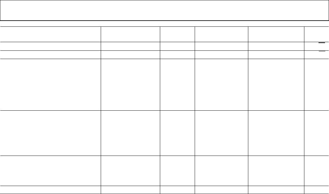
ABSOLUTE MAXIMUM RATINGS
Table 2.
Parameter Rating
Supply Voltage ±18 V
AD811JR Grade Only ±12 V
Internal Power Dissipation Observe Derating Curves
8-Lead PDIP Package θ
JA
= 90°C/ W
8-Lead CERDIP Package θ
JA
= 110°C/W
8-Lead SOIC_N Package θ
JA
= 155°C/W
16-Lead SOIC_W Package θ
JA
= 85°C/W
20-Lead LCC Package θ
JA
= 70°C/W
Output Short-Circuit Duration Observe Derating Curves
Common-Mode Input Voltage ±V
S
Differential Input Voltage ±6 V
Storage Temperature Range (Q, E) −65°C to +150°C
Storage Temperature Range (N, R) −65°C to +125°C
Operating Temperature Range
AD811J 0°C to +70°C
AD811A −40°C to +85°C
AD811S −55°C to +125°C
Lead Temperature Range
(Soldering 60 sec)
300°C
Stresses at or above those listed under Absolute Maximum
Ratings may cause permanent damage to the product. This is a
stress rating only; functional operation of the product at these
or any other conditions above those indicated in the operational
section of this specification is not implied. Operation beyond
the maximum operating conditions for extended periods may
affect product reliability.
MAXIMUM POWER DISSIPATION
The maximum power that can be safely dissipated by the AD811 is
limited by the associated rise in junction temperature. For the
plastic packages, the maximum safe junction temperature is 145°C.
For the CERDIP and LCC packages, the maximum junction tem-
perature is 175°C. If these maximums are exceeded momentarily,
proper circuit operation is restored as soon as the die tempera-
ture is reduced. Leaving the device in the overheated condition
for an extended period can result in device burnout. To ensure
proper operation, it is important to observe the derating curves
in Figure 21 and Figure 24.
While the AD811 is internally short-circuit protected, this may
not be sufficient to guarantee that the maximum junction tem-
perature is not exceeded under all conditions. An important
example is when the amplifier is driving a reverse-terminated
75 Ω cable and the cables far end is shorted to a power supply.
With power supplies of ±12 V (or less) at an ambient temperature
of +25°C or less, and the cable shorted to a supply rail, the
amplifier is not destroyed, even if this condition persists for
an extended period.
METALIZATION PHOTOGRAPH
Contact the factory for the latest dimensions.
Figure 4. Metalization Photograph
Dimensions Shown in Inches and (Millimeters)
ESD CAUTION
0.0618
(1.57)
0.098 (2.49)
+INPUT
INPUT
V–
V+
V
OUT
AD811
6
7
4
3
2
00866-E-007

AD811JRZ

Mfr. #:
Manufacturer:
Analog Devices Inc.
Description:
Video Amplifiers AD811 Eval Brd
Lifecycle:
New from this manufacturer.
Delivery:
DHL FedEx Ups TNT EMS
Payment:
T/T Paypal Visa MoneyGram Western Union