NCP1082
http://onsemi.com
10
Table 3. OPERATING CONDITIONS
Symbol Parameter Conditions Min. Typ. Max. Units
OSCILLATOR
DutyC
Maximum duty cycle Fixed internally 80%
Frange Oscillator frequency range 100 500 kHz
F_acc Oscillator frequency accuracy ±25 %
CURRENT CONSUMPTION
IvportP
1
VPORTP internal current consumption
(Note 12)
DCDC controller off 2.5 3.5 mA
IvportP
2
VPORTP internal current consumption
(Note 13)
DCDC controller on 4.7 6.5 mA
THERMAL SHUTDOWN
TSD
Thermal shutdown threshold T
J
= junction temperature 150 °C T
J
Thyst Thermal hysteresis T
J
= junction temperature 15 °C T
J
THERMAL RATINGS
Ta
Ambient temperature 40 85 °C
Tj Junction temperature Parametric values guaranteed
Max 1000 hours
125
150
°C
°C
12.Conditions
a. No current through the passswitch
b. DCDC controller inactive (SS shorted to RTN)
c. No external load on VDDH and VDDL
d. VPORTP = 57 V
13.Conditions
a. No current through the passswitch
b. Oscillator frequency = 100 kHz
c. No external load on VDDH and VDDL
d. Aux winding not used
e. 2 nF on GATE, DCDC controller enabled
f. VPORTP = 57 V
Figure 6. (Ivddl_load)max with Auxiliary
Supply Operation
Figure 7. (Ivddh_load+Ivddl_load)max with
Auxiliary Supply Operation
VPORTPARTN VOLTAGE DURING PWM OPERA-
TION (V)
VPORTPARTN VOLTAGE DURING PWM OPERA-
TION (V)
131211.51110.5109.08.5
4.0
4.5
5.0
6.5
7.5
8.5
9.5
10.5
0.50
0.75
1.00
1.25
1.75
2.00
2.25
2.50
LOAD CURRENT (mA)
LOAD CURRENT (mA)
9.5 12.5 13.5
5.5
6.0
7.0
8.0
9.0
10.0
131211.51110.5109.08.5 9.5 12.5 13.5
1.50
NCP1082
http://onsemi.com
11
DESCRIPTION OF OPERATION
Powered Device Interface
The PD interface portion of the NCP1082 supports the
IEEE 802.3af defined operating modes: detection signature,
current source classification, inrush and operating current
limits. In order to give more flexibility to the user and also
to keep control of the power dissipation in the NCP1082,
both current limits are configurable. The device enters
operation once its programmable Vuvlo_on threshold is
reached, and operation ceases when the supplied voltage
falls below the Vuvlo_off threshold. Sufficient hysteresis
and Uvlo filter time are provided to avoid false power on/off
cycles due to transient voltage drops on the cable.
Detection
During the detection phase, the incremental equivalent
resistance seen by the PSE through the cable must be in the
IEEE 802.3af standard specification range (23.75 kW to
26.25 kW) for a PSE voltage from 2.7 V to 10.1 V. In order
to compensate for the nonlinear effect of the diode bridge
and satisfy the specification at low PSE voltage, the
NCP1082 presents a suitable impedance in parallel with the
25.5 kW R
det
external resistor connected between VPORTP
and VPORTN. For some types of diodes (especially Schottky
diodes), it may be necessary to adjust this external resistor.
When the Detection_Off level is detected (typically
11.5 V) on VPORTP, the NCP1082 turns on its internal
3.3 V regulator and biasing circuitry in anticipation of the
classification phase as the next step.
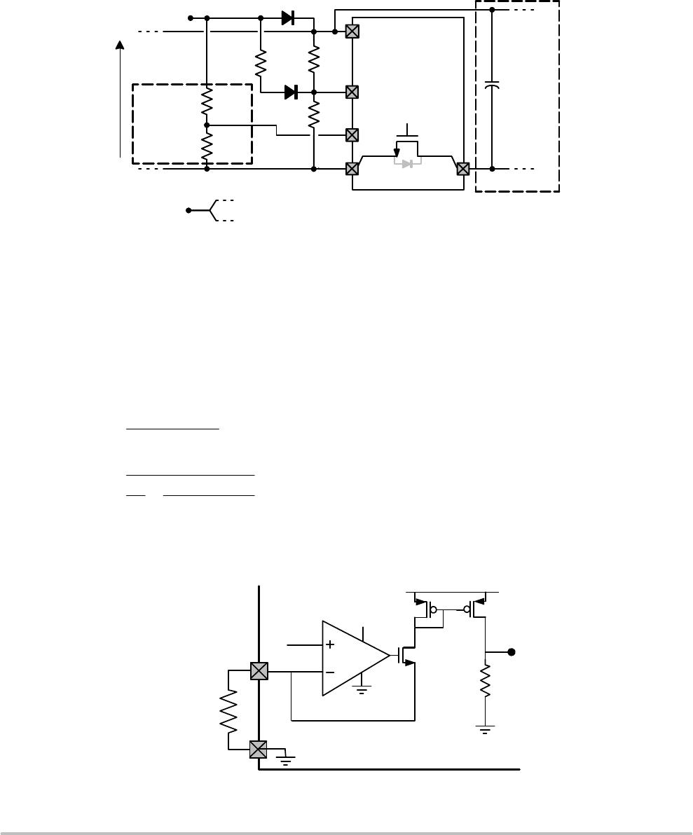
Classification
Once the PSE device has detected the PD device, the
classification process begins. In classification, the PD
regulates a constant current source that is set by the external
resistor RCLASS value on the CLASS pin. Figure 8 shows
the schematic overview of the classification block. The
current source is defined as:
I
class
+
V
bg
R
class
, (where V
bg
is 1.2 V)
CLASS
VDDA1
1.2 V
VPORTP
VPORTN1,2
NCP1082
Rclass
Figure 8. Classification Block Diagram
Power Mode
When the classification handshake is completed, the
PSE and PD devices move into the operating mode.
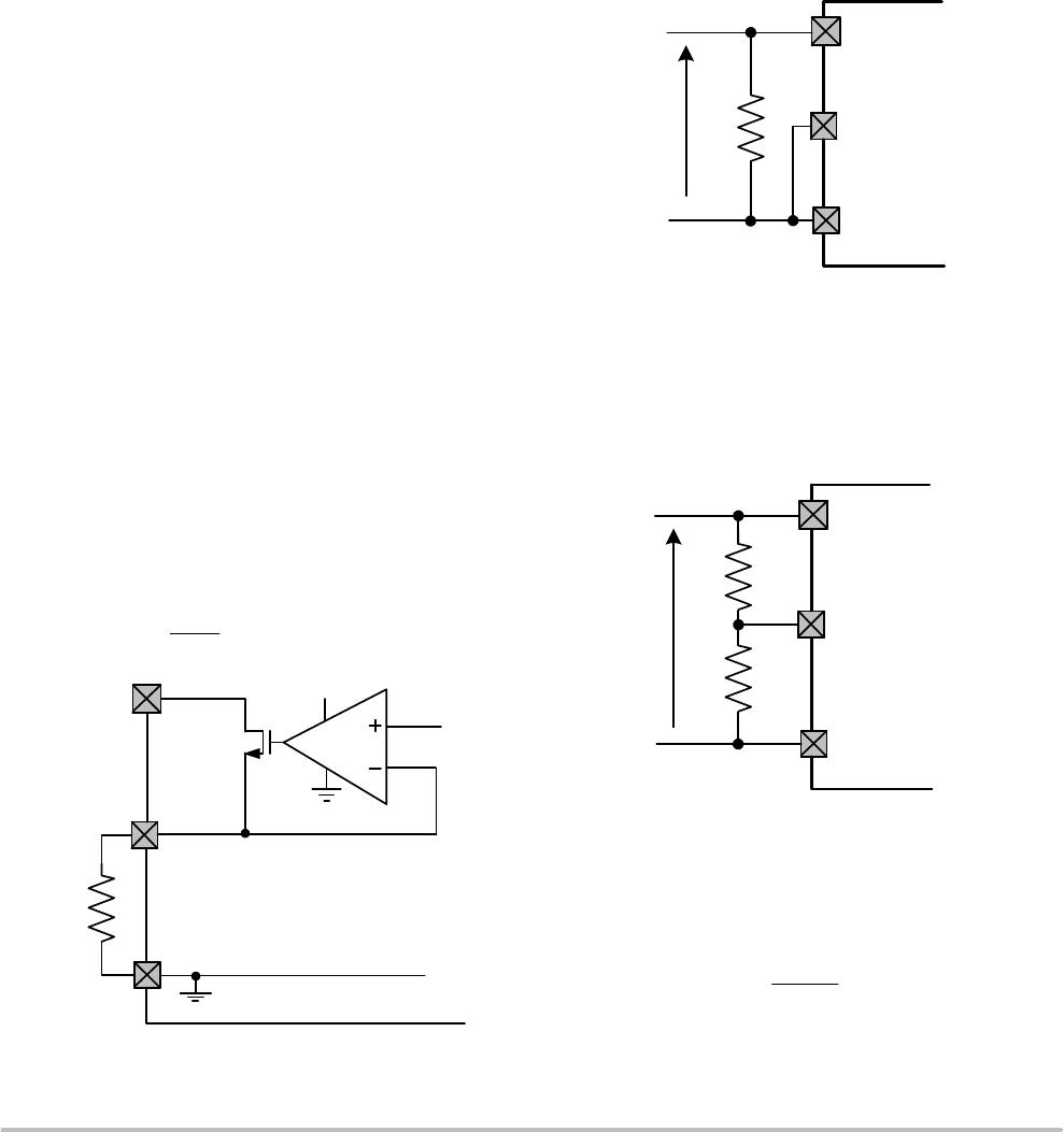
Under Voltage Lock Out (UVLO)
The NCP1082 incorporates an under voltage lock out
(UVLO) circuit which monitors the input voltage and
determines when to apply power to the DCDC controller.
To use the default settings for UVLO (see Table 3), the pin
UVLO must be connected to VPORTN
1,2
. In this case the
signature resistor has to be placed directly between
VPORTP and VPORTN
1,2
, as shown in Figure 9.
Figure 9. Default UVLO Settings
UVLO
VPORTP
VPORTN1,2
NCP1082
VPORT
Rdet
To define the UVLO threshold externally, the UVLO pin
must be connected to the center of an external resistor
divider between VPORTP and VPORTN
1,2
as shown in
Figure 10. The series resistance value of the external
resistors must add to 25.5 kW and replaces the internal
signature resistor.
Figure 10. External UVLO Configuration
UVLO
VPORTN1,2
NCP1082
VPORT
R2
R1
VPORTP
For a Vuvlo_on desired turnon voltage threshold, R1 and
R2 can be calculated using the following equations:
R1 ) R2 + R
det
R2 +
1.2
V
ulvo_on
R
det
When using the external resistor divider, the NCP1082 has
an external reference voltage hysteresis of 15 percent typical.
NCP1082
http://onsemi.com
12
Auxiliary Supply Support
To support applications connected to non PoE enabled
networks and minimize the bill of materials, the NCP1082
supports drawing power from an external supply. The
NCP1082 supports the IEEE 802.3af standard when the PoE
capability is available and acts as a regular DC-DC converter
when there is no power source on the Ethernet cable as
shown in Figure 11.
Auxiliary supply support can be implemented in three
ways depending on where the auxiliary supply is injected.
The front, rear and direct auxiliary supply configurations are
explained in more detail in the application note AND9080.
UVLO
VPORTN1,2
NCP1082
VPORTP
Rdet1
Raux2
VAUX(+)
Rdet2
Pass
Switch
RTN
Raux1
Raux3
AUX
D1
D2
POE(+)
POE()
VPORT
Cpd
DCDC Stage
VAUX()
to VPORTN1,2 (Front AUX Configuration)
to RTN (Rear AUX Configuration)
Or
Figure 11. Front and Rear Auxiliary Supply Input with Support for Very Low Input Voltages
Optional
for very low
VAUX only
When the auxiliary input supply is above 13.5 V, connect
the AUX pin to VPORTN
1,2.
. When the auxiliary supply is
below 13.5 V (but above 9 V), calculate the voltage dividers
Raux1, Raux3 and Raux2, Rdet1, Rdet2 to divide the input
voltage using the below formulas together with the formulas
from the previous section. This will ensure that for valid input
voltages, the voltage at the UVLO and AUX pins are above
their threshold voltages. Note that the maximum voltage is
3.3 V.
R
aux3
+
R
aux1
V
t
V
aux
* V
dp
* V
t
R
aux1
+ 20 kW
R
aux2
+
V
aux
* V
dp
* V
d
* V
t
V
t
845
*
V
aux
*V
dp
*V
d
*V
t
24 K
Where V
d
is the voltage drop over the rectifiers and masking
diodes (typical 0.6 V), V
dp
is the forward drop of the
NCP1082 internal diode (typical 0.5 V), and V
t
is the
threshold voltage on the AUX pin (typical 1.5 V).
Note that as soon the auxiliary supply is connected the
PoE interface (detection and classification) is disabled and
does not allow the PD device to be powered from the
Ethernet until the auxiliary supply is removed.
If the PoE PD device was drawing the current from the
Ethernet cable before the auxiliary supply is connected, the
power will continue to be supplied from the Ethernet cable
unless the voltage of the auxiliary supply is higher than the
Ethernet supply voltage.
Inrush and Operational Current Limitations
The inrush current limit and the operational current limit
are programmed individually by an external Rinrush and
Rilim1 resistors respectively connected between INRUSH
and VPORTN
1,2
, and between ILIM1 and VPORTN
1,2
as
shown in Figure 12.
ILIM1 /
INRUSH
VDDA1
Vbg1
VDDA1
VPORTNx
Ilim_ref
NCP1082
Figure 12. Current Limitation Configuration (Inrush & Ilim1 Pins)

NCP1082DER2G

Mfr. #:
Manufacturer:
ON Semiconductor
Description:
Switching Controllers POE-PD 13W DC-DC AUX SUPP
Lifecycle:
New from this manufacturer.
Delivery:
DHL FedEx Ups TNT EMS
Payment:
T/T Paypal Visa MoneyGram Western Union

Products related to this Datasheet