NCP1082
http://onsemi.com
4
SIMPLIFIED APPLICATION DIAGRAMS
Figure 4. NonIsolated Flyback with Extra Winding and Rear Auxiliary Support
NCP1082
Rcs
Cvddl
Cvddh
Cpd
Css
Rosc
M1
T1
Cload
LD1
Rd1
Rclass
Rilim1
Rinrush
Rslope
Voutput
D1
GATE
RTN
FB
VPORTN2
VDDH
VDDL
VPORTN1
CLASS
ARTN
ILIM1
INRUSH
TEST
AUX
UVLO
CS
VPORTP
Data
Pairs
Spare
Pairs
R1
R2
RJ45
DB1
DB2
Raux1
VAUX(+)
VAUX()
Raux2
Raux3
D3
D4
Cline
Z_line
COMPSS OSC
R3
R4
C1comp
C2comp
Rcomp
R5
D2
Figure 4 shows the same nonisolated flyback configuration as Figure 3, but adds a 12 V auxiliary bias winding on the
transformer to provide power to the NCP1082 DCDC controller via its VDDH pin. This topology shuts off the current flowing
from VPORTP to VDDH and therefore reduces the internal power dissipation of the PD, resulting in higher overall power
efficiency.
Figure 5. NonIsolated Forward Converter with Rear Auxiliary Support
NCP1082
Rcs
Cvddl
Cvddh
Cpd
Css
Rosc
M1
T1
Cload
LD1
Rd1
Rclass
Rilim1
Rinrush
Rslope
VoutputD1
GATE
RTN
FB
VPORTN2
VDDH
VDDL
VPORTN1
CLASS
ARTN
ILIM1
INRUSH
TEST
AUX
UVLO
CS
VPORTP
Data
Pairs
Spare
Pairs
R1
R2
RJ45
DB1
DB2
Raux1
VAUX(+)
VAUX()
Raux2
Raux3
D4
D5
Cline
Z_line
COMPSS OSC
R3
R4
C1comp
C2comp
Rcomp
D3
D2
L1
Figure 5 shows the NCP1082 used in a nonisolated forward topology.
NCP1082
http://onsemi.com
5
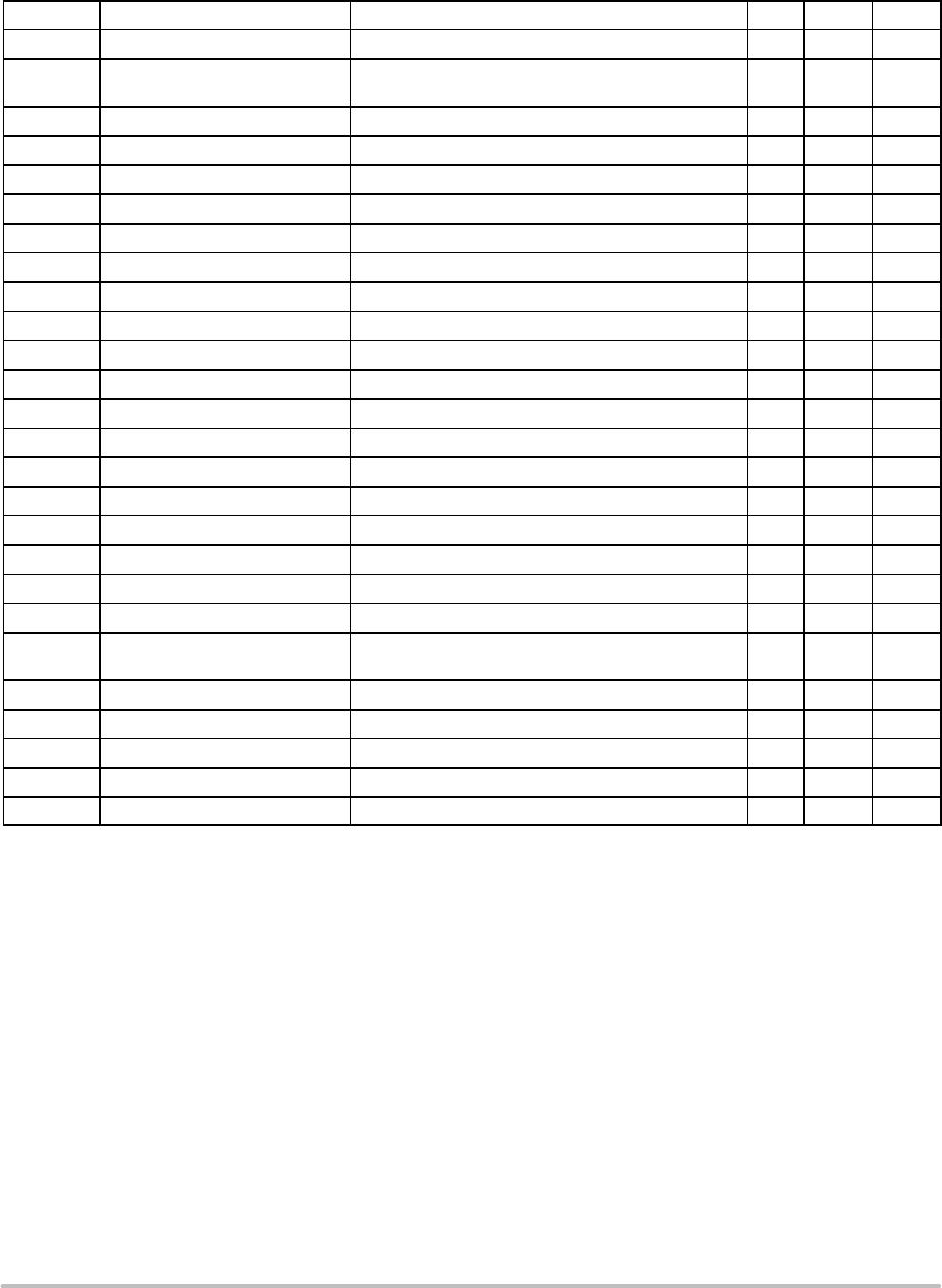
Table 1. PIN DESCRIPTIONS
Name Pin No. Type Description
VPORTP 1 Supply Positive input power. Voltage with respect to VPORTN
1,2
VPORTN1
VPORTN2
6,8 Ground Negative input power. Connected to the source of the internal passswitch.
RTN 7 Ground DCDC controller power return. Connected to the drain of the internal passswitch. It must
be connected to ARTN. This pin is also the drain of the internal passswitch.
ARTN 14 Ground DCDC controller ground pin. Must be connected to RTN as a single point ground connection
for improved noise immunity.
VDDH 16 Supply Output of the 9 V LDO internal regulator. Voltage with respect to ARTN. Supplies the internal
gate driver. VDDH must be bypassed to ARTN with a 1 mF or 2.2 mF ceramic capacitor with
low ESR.
VDDL 17 Supply Output of the 3.3 V LDO internal regulator. Voltage with respect to ARTN. This pin can be
used to bias an external lowpower LED (1 mA max.) connected to ARTN, and can also be
used to add extra biasing current in the external optocoupler. VDDL must be bypassed to
ARTN with a 330 nF or 470 nF ceramic capacitor with low ESR.
CLASS 2 Input Classification current programming pin. Connect a resistor between CLASS and VPORTN
1,2
.
INRUSH 4 Input Inrush current limit programming pin. Connect a resistor between INRUSH and VPORTN
1,2
.
ILIM1 5 Input Operational current limit programming pin. Connect a resistor between ILIM1 and
VPORTN
1,2
.
UVLO 3 Input DCDC controller undervoltage lockout input. Voltage with respect to VPORTN
1,2
. Connect
a resistordivider from VPORTP to UVLO to VPORTN
1,2
to set an external UVLO threshold.
GATE 15 Output DCDC controller gate driver output pin.
OSC 11 Input Internal oscillator frequency programming pin. Connect a resistor between OSC and ARTN.
NC 13 No connect pin, must not be connected.
COMP 18 I/O Output of the internal error amplifier of the DCDC controller. COMP is pulledup internally to
VDDL with a 5 kW resistor. In isolated applications, COMP is connected to the collector of the
optocoupler. Voltage with respect to ARTN.
FB 19 Input DCDC controller inverting input of the internal error amplifier. In isolated applications, the pin
should be strapped to ARTN to disable the internal error amplifier.
CS 12 Input Currentsense input for the DCDC controller. Voltage with respect to ARTN.
SS 20 Input Softstart input for the DCDC controller. A capacitor between SS and ARTN determines the
softstart timing.
AUX 9 Input When the pin is pulled up, the IEEE detection mode is disabled and the device can be sup-
plied by an auxiliary supply. Voltage with respect to VPORTN
1,2
. Connect the pin to the auxili-
ary supply through a resistor divider.
TEST 10 Input Digital test pin must always be connected to VPORTN
1,2
.
EP Exposed pad. Connected to VPORTN
1,2
ground.
NCP1082
http://onsemi.com
6
Table 2. ABSOLUTE MAXIMUM RATINGS
Symbol Parameter Conditions Min Max Unit
VPORTP Input power supply Voltage with respect to VPORTN
1,2
0.3 72 V
RTN
ARTN
Analog ground supply 2 Passswitch in offstate
(Voltage with respect to VPORTN
1,2
)
0.3 72 V
VDDH Internal regulator output Voltage with respect to ARTN 0.3 17 V
VDDL Internal regulator output Voltage with respect to ARTN 0.3 3.6 V
CLASS Analog output Voltage with respect to VPORTN
1,2
0.3 3.6 V
INRUSH Analog output Voltage with respect to VPORTN
1,2
0.3 3.6 V
ILIM1 Analog output Voltage with respect to VPORTN
1,2
0.3 3.6 V
UVLO Analog input Voltage with respect to VPORTN
1,2
0.3 3.6 V
OSC Analog output Voltage with respect to ARTN 0.3 3.6 V
COMP Analog input / output Voltage with respect to ARTN 0.3 3.6 V
FB Analog input Voltage with respect to ARTN 0.3 3.6 V
CS Analog input Voltage with respect to ARTN 0.3 3.6 V
SS Analog input Voltage with respect to ARTN 0.3 3.6 V
NC Open pin
AUX Analog input Voltage with respect to VPORTN
1,2
0.3 3.6 V
TEST Digital input Voltage with respect to VPORTN
1,2
0.3 3.6 V
T
A
Ambient temperature 40 85 °C
T
J
Junction temperature 150 °C
T
J
TSD Junction temperature (Note 1) Thermal shutdown condition 175 °C
T
stg
Storage Temperature 55 150 °C
T
θ
JA
Thermal Resistance,
Junction to Air (Note 2)
Exposed pad connected to VPORTN
1,2
ground 37.6 °C/W
ESDHBM Human Body Model per JEDEC Standard JESD22 4 kV
ESDCDM Charged Device Model 750 V
ESDMM Machine Model 300 V
LU Latchup per JEDEC Standard JESD78 ±200 mA
ESDSYS System ESD (contact/air) (Note 3) 8/15 kV
Stresses exceeding Maximum Ratings may damage the device. Maximum Ratings are stress ratings only. Functional operation above the
Recommended Operating Conditions is not implied. Extended exposure to stresses above the Recommended Operating Conditions may affect
device reliability.
1. T
J
TSD allowed during error conditions only. It is assumed that this maximum temperature condition does not occur more than 1 hour
cumulative during the useful life for reliability reasons.
2. Mounted on a 1S2P (3 layer) test board with copper coverage of 25 percent for the signal layers and 90 percent copper coverage for the
inner planes at an ambient temperature of 85°C in still air. Refer to JEDEC JESD517 for details.
3. Surges per EN6100042, 1999 applied between RJ45 and output ground and between adapter input and output ground of the demo board.
The specified values are the test levels and not the failure levels.

NCP1082DER2G

Mfr. #:
Manufacturer:
ON Semiconductor
Description:
Switching Controllers POE-PD 13W DC-DC AUX SUPP
Lifecycle:
New from this manufacturer.
Delivery:
DHL FedEx Ups TNT EMS
Payment:
T/T Paypal Visa MoneyGram Western Union

Products related to this Datasheet