16
LTC1416
APPLICATIONS INFORMATION
WUU
U
Figure 14a. Suggested Evaluation Circuit Schematic
+
+V
IN
GND
A
+
A
AGND
DGND
V
CC
V
CC
V
CC
V
SS
V
REF
JP4
V
LOGIC
R14
20
U4
LTC1416
B[00:13]
U5
74HC574
U6
74HC574
98
HC14
U7D
J6-13
J6-14
J6-11
J6-12
J6-9
J6-10
J6-7
J6-8
J6-5
J6-6
J6-3
J6-4
J6-1
J6-2
J6-15
J6-16
J6-17
J6-18
D13
D00
D01
D02
D03
D04
D05
D06
D07
D08
D09
D10
D11
D12
D13
D13
RDY
D00
D01
D02
D03
D04
D05
D06
D07
D08
D09
D10
D11
D12
D13
D13
RDY
DGND
DGND
LED
JP1
D00
D01
D02
D03
D04
D05
D06
D07
D08
D09
D10
D11
D12
D13
D00
D01
D02
D03
D04
D05
D06
D07
D08
D09
D10
D11
D12
D13
D0
D1
D2
D3
D4
D5
D6
D7
D8
D9
D10
D11
D12
D13
D[00:13]
R0, 1.2k
R1, 1.2k
R2, 1.2k
R3, 1.2k
R4, 1.2k
R5, 1.2k
R6, 1.2k
R8, 1.2k
R7, 1.2k
R9, 1.2k
R10, 1.2k
R11, 1.2k
R12, 1.2k
R13, 1.2k
HEADER
18-PIN
11 10
HC14
R21
1k
V
LOGIC
V
CC
GND
D0
D1
D2
D3
D4
D5
D6
D7
D0
D1
D2
D3
D4
D5
D6
D7
D12
D11
D10
D09
D08
D07
D06
D00
D01
D02
D03
D04
D05
D13
19
18
17
16
15
14
13
12
19
18
17
16
15
14
13
12
Q0
Q1
Q2
Q3
Q4
Q5
Q6
Q7
Q0
Q1
Q2
Q3
Q4
Q5
Q6
Q7
0E
0E
DATA READY
NOTES: UNLESS OTHERWISE SPECIFIED
ALL RESISTOR VALUES IN OHMS, 5%
V
CC
V
SS
CLK
J7
V
IN
U2 LT1121-5
D15
SS12
R17
10k
R18
10k
R19
51
R16
51
R15
51
JP5C
RD
SHDN
CS
HC14 HC14
C11
1000pF
C8
1µF
10V
C13
22µF
10 V
C9
10µF
10V
C6
15pF
C5
10µF
10V
C2
22µF
10V
C10
10µF
10V
C1
22µF
10V
C12
0.1µF
C14
0.1µF
GND TABGND
1
24
3
C4
0.1µF
C3
0.1µF
U3
LT1363
V
V
+
2
3
1
23
4
6
7
8
1
4
J3
7V TO
15V
J4
JP2
J5
JP3
V
OUT
V
OUT
J2
1
2
3
4
25
24
23
22
21
28
27
26
5
14
6
7
8
9
10
11
12
13
15
16
17
18
19
20
B13
B12
B11
B10
B09
B08
B07
B06
B05
B04
B03
B02
B01
B00
B12
B11
B10
B09
B08
B07
B06
1
11
2
3
4
5
6
7
8
9
1
11
2
3
4
5
6
7
8
9
D13
D12
D11
D10
D9
D8
D7
D6
D5
D4
D3
D2
D1
D0
A
IN
+
A
IN
V
REF
REFCOMP
BUSY
CS
CONVST
RD
SHDN
AV
DD
DV
DD
V
SS
AGND
DGND
JP5B
JP5A
R20
1M
V
LOGIC
14
7
13
12
U7F
HC14
+
+
V
SS
J1
7V TO
15V
D14
SS12
–V
IN
2
5
1
U1
79L05
+
1416 F14a
V
IN
V
OUT
GND
U7G
HC14
U7B
U7A
U7E
C15
0.1µF
56
HC14
U7C
17
LTC1416
APPLICATIONS INFORMATION
WUU
U
Figure 14b. Suggested Evaluation Circuit Board—
Component Side Silkscreen
Figure 14c. Suggested Evaluation Circuit Board—
Component Side Layout
Figure 14d. Suggested Evaluation Circuit Board—
Solder Side Layout
t
4
SHDN
CONVST
1416 F15b
Figure 15b. SHDN to CONVST Wake-Up Timing
t
3
CS
SHDN
1416 F15a
Figure 15a. CS to SHDN Timing
18
LTC1416
APPLICATIONS INFORMATION
WUU
U
Shutdown is controlled by Pin 21 (SHDN), the ADC is in
shutdown when it is low. The shutdown mode is selected
with Pin 20 (CS), low selects nap.
Timing and Control
Conversion start and data read operations are controlled
by three digital inputs: CONVST, CS and RD. A logic “0”
applied to the CONVST pin will start a conversion after the
ADC has been selected (i.e., CS is low). Once initiated, it
cannot be restarted until the conversion is complete.
Converter status is indicated by the BUSY output. BUSY is
low during a conversion.
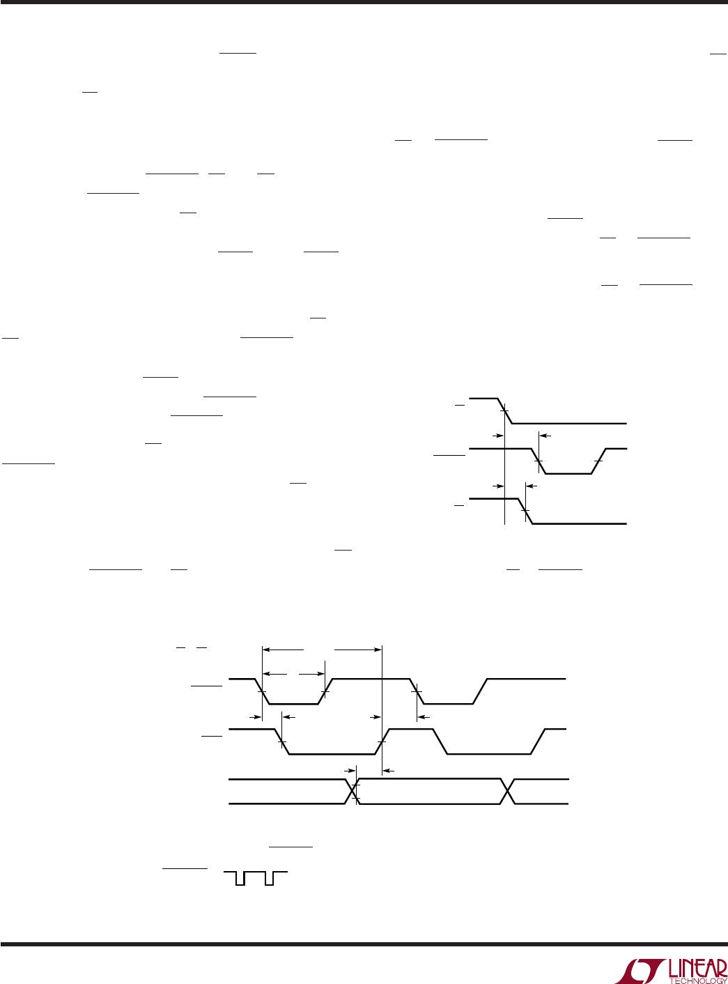
Figures 16 through 21 show several different modes of
operation. In modes 1a and 1b (Figures 17 and 18), CS and
RD are both tied low. The falling edge of CONVST starts the
conversion. The data outputs are always enabled and data
can be latched with the BUSY rising edge. Mode 1a shows
operation with a narrow logic low CONVST pulse. Mode 1b
shows a narrow logic high CONVST pulse.
In mode 2 (Figure 19), CS is tied low. The falling edge of
CONVST signal again starts the conversion. Data outputs
are in three-state until read by the MPU with the RD signal.
Mode 2 can be used for operation with a shared MPU data
bus.
In slow memory and ROM modes (Figures 20 and 21), CS
is tied low and CONVST and RD are tied together. The MPU
Figure 16. CS to CONVST Setup Timing
DATA N
DB13 TO DB0
DATA (N + 1)
DB13 TO DB0
DATA (N – 1)
DB13 TO DB0
CONVST
CS = RD = 0
BUSY
1416 F17
t
5
t
CONV
t
6
t
8
t
7
DATA
(SAMPLE N)
(CONVST = )
Figure 17. Mode 1a. CONVST Starts a Conversion. Data Outputs Always Enabled
starts the conversion and reads the output with the RD
signal. Conversions are started by the MPU or DSP (no
external sample clock).
In slow memory mode, the processor applies a logic low
to RD (=CONVST), starting the conversion. BUSY goes
low, forcing the processor into a Wait state. The previous
conversion result appears on the data outputs. When the
conversion is complete, the new conversion results
appear on the data outputs; BUSY goes high releasing the
processor, and the processor takes RD (=CONVST) back
high and reads the new conversion data.
In ROM mode, the processor takes RD (=CONVST) low,
starting a conversion and reading the previous conversion
result. After the conversion is complete, the processor can
read the new result and initiate another conversion.

LTC1416CG#PBF

Mfr. #:
Manufacturer:
Analog Devices Inc.
Description:
Analog to Digital Converters - ADC 400ksps 14-Bit Parallel ADC
Lifecycle:
New from this manufacturer.
Delivery:
DHL FedEx Ups TNT EMS
Payment:
T/T Paypal Visa MoneyGram Western Union