4
LTC1416
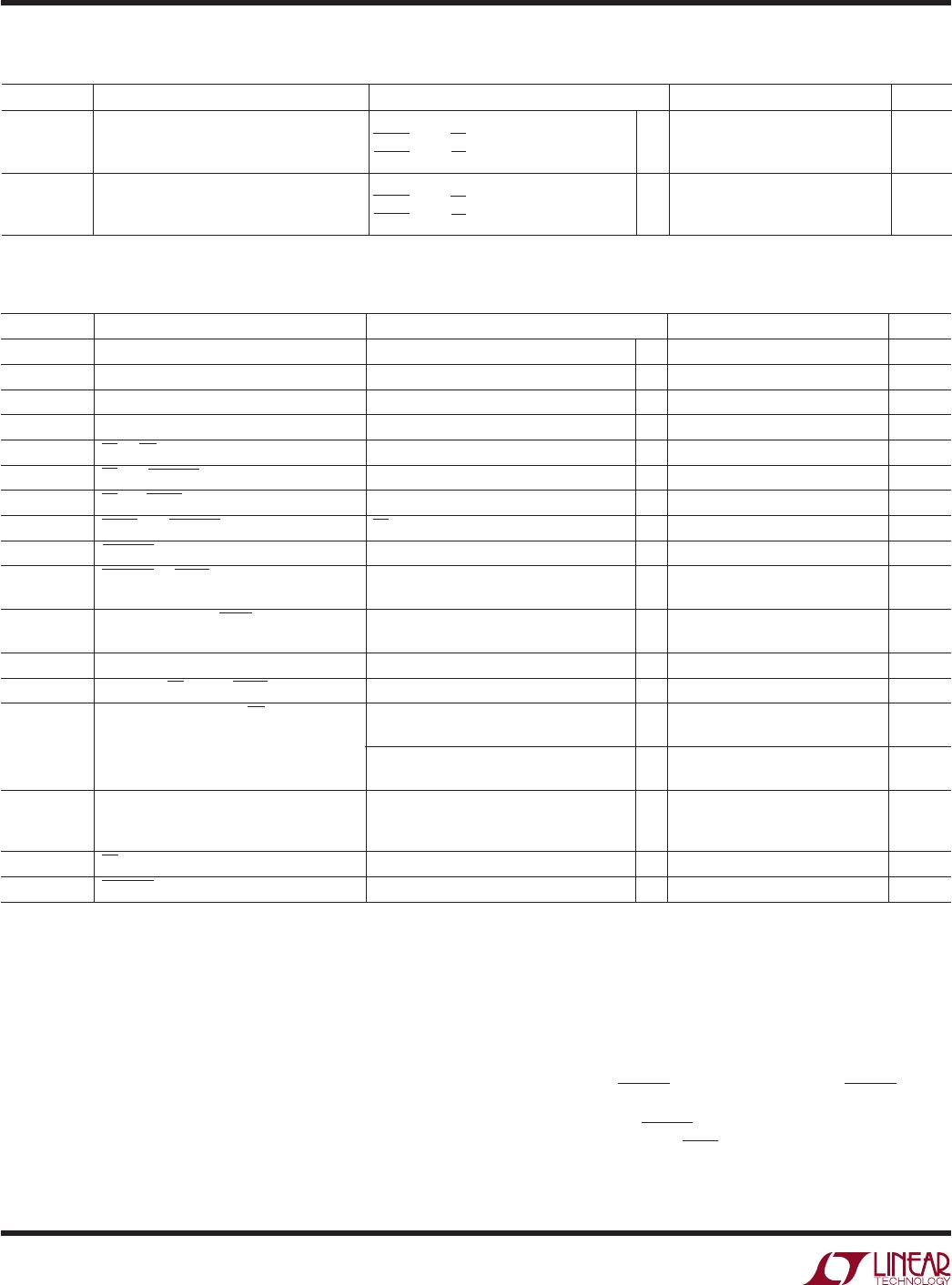
SYMBOL PARAMETER CONDITIONS MIN TYP MAX UNITS
f
SAMPLE(MAX)
Maximum Sampling Frequency 400 kHz
t
CONV
Conversion Time 1.5 1.9 2.2 µs
t
ACQ
Acquisition Time (Note 9) 100 400 ns
t
ACQ+CONV
Acquisition + Conversion Time 2 2.5 µs
t
1
CS to RD Setup Time (Notes 9, 10) 0ns
t
2
CS to CONVSTSetup Time (Notes 9, 10) 10 ns
t
3
CSto SHDNSetup Time (Notes 9, 10) 10 ns
t
4
SHDN to CONVST Wake-Up Time CS = 0V (Note 10) 400 ns
t
5
CONVST Low Time (Notes 10, 11) 40 ns
t
6
CONVST to BUSY Delay C
L
= 25pF 25 ns
50 ns
t
7
Data Ready Before BUSY (Note 9) 75 100 ns
50 ns
t
8
Delay Between Conversions (Note 10) 40 ns
t
9
Wait Time RD After BUSY –5 ns
t
10
Data Access Time After RD C
L
= 25pF 15 25 ns
35 ns
C
L
= 100pF 20 35 ns
50 ns
t
11
Bus Relinquish Time 820 ns
0°C T
A
70°C 25 ns
–40°C T
A
85°C 30 ns
t
12
RD Low Time t
10
ns
t
13
CONVST High Time 40 ns
Note 7: Integral nonlinearity is defined as the deviation of a code from a
straight line passing through the actual endpoints of the transfer curve.
The deviation is measured from the center of the quantization band.
Note 8: Bipolar offset is the offset voltage measured from –0.5LSB when
the output code flickers between 0000 0000 0000 00 and
1111 1111 1111 11.
Note 9: Guaranteed by design, not subject to test.
Note 10: Recommended operating conditions.
Note 11: The falling CONVST edge starts a conversion. If CONVST returns
high at a critical point during the conversion it can create small errors. For
best results ensure that CONVST returns high either within 900ns after the
start of the conversion or after BUSY rises.
Note 1: Absolute Maximum Ratings are those values beyond which the life
of a device may be impaired.
Note 2: All voltage values are with respect to ground with DGND and
AGND wired together unless otherwise noted.
Note 3: When these pin voltages are taken below V
SS
or above V
DD
, they
will be clamped by internal diodes. This product can handle input currents
greater than 100mA below V
SS
or above V
DD
without latchup.
Note 4: When these pin voltages are taken below V
SS
, they will be clamped
by internal diodes. This product can handle input currents greater than
100mA below V
SS
without latchup. These pins are not clamped to V
DD
.
Note 5: V
DD
= 5V, V
SS
= –5V, f
SAMPLE
= 400kHz, t
r
= t
f
= 5ns unless
otherwise specified.
Note 6: Linearity, offset and full-scale specifications apply for a single-
ended A
IN
+
input with A
IN
grounded.
POWER REQUIRE E TS
WU
SYMBOL PARAMETER CONDITIONS MIN TYP MAX UNITS
I
SS
Negative Supply Current 710 mA
Nap Mode SHDN = 0V, CS = 0V 20 µA
Sleep Mode SHDN = 0V, CS = 5V 15 µA
P
DISS
Power Dissipation 70 100 mW
Power Dissipation, Nap Mode SHDN = 0V, CS = 0V 4 6 mW
Power Dissipation, Sleep Mode SHDN = 0V, CS = 5V 0.1 mW
The denotes specifications which apply over the full operating temperature range,
otherwise specifications are at T
A
= 25°C. (Note 5)
TI I G CHARACTERISTICS
UW
The denotes specifications which apply over the full operating temperature
range, otherwise specifications are at T
A
= 25°C. (Note 5, see Figures 15 to 21)
5
LTC1416
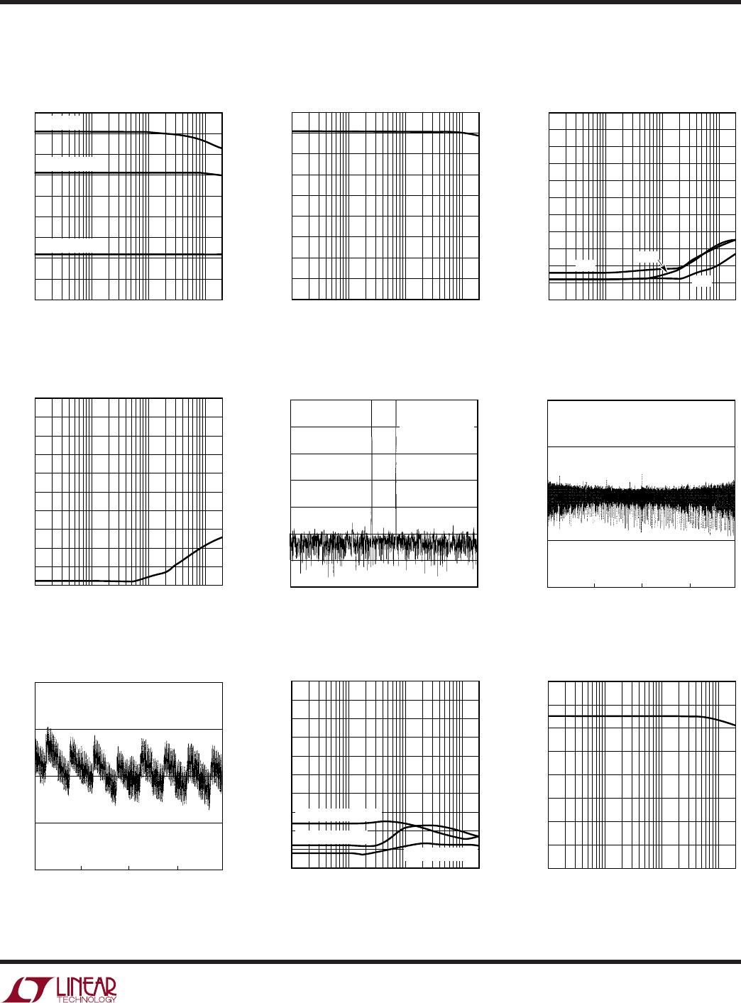
TYPICAL PERFORMANCE CHARACTERISTICS
UW
Distortion vs Input Frequency
Differential Nonlinearity
vs Output Code
Input Common Mode Rejection
vs Input Frequency
INPUT FREQUENCY (Hz)
1k
SIGNAL/(NOISE + DISTORTION) (dB)
90
80
70
60
50
40
30
20
10
0
10k 100k
1416 G01
1M 2M
V
IN
= 0dB
V
IN
= –20dB
V
IN
= –60dB
S/(N + D) vs Input Frequency
and Amplitude
INPUT FREQUENCY (Hz)
1k
SPURIOUS-FREE DYNAMIC RANGE (dB)
0
–10
–20
–30
–40
–50
–60
–70
–80
–90
100
10k 100k
1416 G04
1M 2M
Spurious-Free Dynamic Range
vs Input Frequency
OUTPUT CODE
0
DNL ERROR (LSB)
16384
V
OUT
= ±2.5V
V
REF
= 2.5V
1416 G06
4096
8192
12288
1.0
0.5
0
0.5
1.0
OUTPUT CODE
0
INL ERROR (LSB)
16384
V
OUT
= ±2.5V
V
REF
= 2.5V
1416 G07
4096
8192
12288
1.0
0.5
0
0.5
1.0
Integral Nonlinearity
vs Output Code
INPUT FREQUENCY (Hz)
1k
COMMON MODE REJECTION (dB)
80
70
60
50
40
30
20
10
0
10k 100k
1416 G09
1M 2M
INPUT FREQUENCY (Hz)
1k
AMPLITUDE (dB BELOW THE FUNDAMENTAL)
0
–10
–20
–30
–40
–50
–60
–70
–80
–90
100
110
10k 100k
1416 G03
1M 2M
THD
2ND
3RD
Signal-to-Noise Ratio
vs Input Frequency
Intermodulation Distortion Plot
Power Supply Feedthrough
vs Ripple Frequency
INPUT FREQUENCY (Hz)
1k
SIGNAL-TO-NOISE RATIO (dB)
90
80
70
60
50
40
30
20
10
0
10k 100k
1416 G02
1M 2M
FREQUENCY (Hz)
0
AMPLITUDE (dB)
0
–20
–40
–60
–80
100
120
140
20
100
140
1416 G05
80
180
200
40
60
120 160
f
SAMPLE
= 400kHz
f
a
=87.01171876kHz
f
b
=113.1835938kHz
RIPPLE FREQUENCY (Hz)
1k
AMPLITUDE OF
POWER SUPPLY FEEDTHROUGH (dB)
0
–10
–20
–30
–40
–50
–60
–70
–80
–90
100
10k 100k
1416 G08
1M 2M
DGND (V
IN
= 100mV)
V
SS
(V
IN
= 10mV)
V
DD
(V
IN
= 10mV)
6
LTC1416
PI FU CTIO S
UU U
A
IN
+
(Pin 1): ±2.5V Positive Analog Input.
A
IN
(Pin 2): ±2.5V Negative Analog Input.
V
REF
(Pin 3): 2.5V Reference Output. Bypass to AGND
with 1µF.
REFCOMP (Pin 4): 4.06V Reference Output. Bypass to
AGND with 22µF tantalum in parallel with 0.1µF
ceramic, or 22µF ceramic.
AGND (Pin 5): Analog Ground.
D13 to D6 (Pins 6 to 13): Three-State Data Outputs.
DGND (Pin 14): Digital Ground for Internal Logic. Tie to
AGND.
D5 to D0 (Pins 15 to 20): Three-State Data Outputs.
SHDN (Pin 21): Power Shutdown Input. Low selects
shutdown. Shutdown mode selected by CS. CS = 0 for
nap mode and CS = 1 for sleep mode.
RD (Pin 22): Read Input. This enables the output
drivers when CS is low.
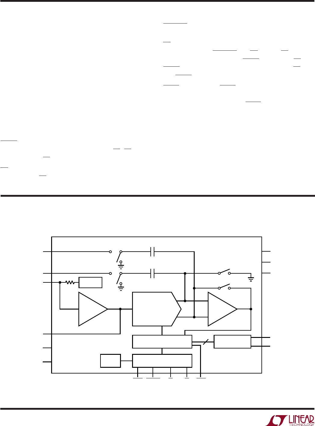
FU CTIO AL BLOCK DIAGRA
UU W
CONVST (Pin 23): Conversion Start Signal. This active
low signal starts a conversion on its falling edge.
CS (Pin 24): The Chip Select input must be low for the
ADC to recognize CONVST and RD inputs. CS also sets
the shutdown mode when SHDN goes low. CS and
SHDN low select the quick wake-up nap mode. CS high
and SHDN low select sleep mode.
BUSY (Pin 25): The BUSY output shows the converter
status. It is low when a conversion is in progress. Data
is valid on the rising edge of BUSY.
V
SS
(Pin 26):5V Negative Supply. Bypass to AGND
with 10µF tantalum in parallel with 0.1µF ceramic, or
10µF ceramic.
DV
DD
(Pin 27): 5V Positive Supply. Tie to Pin 28.
AV
DD
(Pin 28): 5V Positive Supply. Bypass to AGND
with 10µF tantalum in parallel with 0.1µF ceramic, or
10µF ceramic.
14-BIT CAPACITIVE DAC
COMPREF AMP
2.5V REF
4k
REFCOMP
(4.06V)
C
SAMPLE
C
SAMPLE
D13
D0
BUSY
CONTROL LOGIC
CSCONVST RDSHDN
INTERNAL
CLOCK
ZEROING SWITCHES
DV
DD
V
SS
AV
DD
A
IN
+
A
IN
V
REF
AGND
DGND
14
1416 BD
+
SUCCESSIVE APPROXIMATION
REGISTER
OUTPUT LATCHES

LTC1416CG#PBF

Mfr. #:
Manufacturer:
Analog Devices Inc.
Description:
Analog to Digital Converters - ADC 400ksps 14-Bit Parallel ADC
Lifecycle:
New from this manufacturer.
Delivery:
DHL FedEx Ups TNT EMS
Payment:
T/T Paypal Visa MoneyGram Western Union