7
LTC1416
TEST CIRCUITS
1k C
L
C
L
DBN
(A) Hi-Z TO V
OH
AND V
OL
TO V
OH
(B) Hi-Z TO V
OL
AND V
OH
TO V
OL
DBN
1k
5V
1416 TC01
Load Circuits for Access Timing Load Circuits for Output Float Delay
1k 100pF 100pF
DBN
(A) V
OH
TO Hi-Z (B) V
OL
TO Hi-Z
DBN
1k
5V
1416 TC02
APPLICATIONS INFORMATION
WUU
U
CONVERSION DETAILS
The LTC1416 uses a successive approximation algorithm
and an internal sample-and-hold circuit to convert an
analog signal to a 14-bit parallel output. The ADC is
complete with a precision reference and an internal clock.
The control logic provides easy interface to microproces-
sors and DSPs. (Please refer to the Digital Interface
section for the data format.)
Conversion start is controlled by the CS and CONVST
inputs. At the start of the conversion, the successive
approximation register (SAR) is reset. Once a conversion
cycle has begun, it cannot be restarted.
During the conversion, the internal differential 14-bit
capacitive DAC output is sequenced by the SAR from the
most significant bit (MSB) to the least significant bit
(LSB). Referring to Figure 1, the A
IN
+
and A
IN
inputs are
connected to the sample-and-hold capacitors (C
SAMPLE
)
during the acquire phase and the comparator offset is
nulled by the zeroing switches. In this acquire phase, a
minimum delay of 400ns will provide enough time for the
sample-and-hold capacitors to acquire the analog signal.
During the convert phase the comparator zeroing switches
open, putting the comparator into compare mode. The
input switches connect the C
SAMPLE
capacitors to ground,
transferring the differential analog input charge onto the
summing junction. This input charge is successively com-
pared with the binary-weighted charges supplied by the
differential capacitive DAC. Bit decisions are made by the
high speed comparator. At the end of a conversion, the
differential DAC output balances the A
IN
+
and A
IN
input
charges. The SAR contents (a 14-bit data word) which
represents the difference of A
IN
+
and A
IN
are loaded into
the 14-bit output latches.
SAMPLE
SAMPLE
C
SAMPLE
+
C
SAMPLE
V
DAC
V
DAC
+
D13
D0
ZEROING SWITCHES
A
IN
+
C
DAC
+
C
DAC
A
IN
14
1416 F01
COMP
+
HOLD
HOLD
HOLD
HOLD
OUTPUT
LATCH
SAR
Figure 1. Simplified Block Diagram
8
LTC1416
APPLICATIONS INFORMATION
WUU
U
Figure 3. Effective Bits and Signal/(Noise + Distortion)
vs Input Frequency
DYNAMIC PERFORMANCE
The LTC1416 has excellent high speed sampling capabil-
ity. FFT (Fast Fourier Transform) test techniques are used
to test the ADC’s frequency response, distortion and noise
at the rated throughput. By applying a low distortion sine
wave and analyzing the digital output using an FFT algo-
rithm, the ADC’s spectral content can be examined for
frequencies outside the fundamental. Figure 2 shows a
typical LTC1416 FFT plot.
Signal-to-Noise Ratio
The Signal-to-Noise plus Distortion Ratio [S/(N + D)] is the
ratio between the RMS amplitude of the fundamental input
frequency to the RMS amplitude of all other frequency
components at the A/D output. The output is band limited
to frequencies from above DC and below half the sampling
frequency. Figure 2a shows a typical spectral content with
a 400kHz sampling rate and a 100kHz input. The dynamic
performance is excellent for input frequencies up to and
beyond the Nyquist limit of 200kHz, Figure 2b.
Effective Number of Bits
The Effective Number of Bits (ENOBs) is a measurement of
the resolution of an ADC and is directly related to the
S/(N + D) by the equation:
ENOB = [S/(N + D) – 1.76]/6.02
where ENOB is the Effective Number of Bits of resolution
and S/(N + D) is expressed in dB. At the maximum
sampling rate of 400kHz, the LTC1416 maintains near
ideal ENOBs up to the Nyquist input frequency of 200kHz
(refer to Figure 3).
FREQUENCY (kHz)
0
AMPLITUDE (dB)
150
1416 F02a
50 100 200
0
–20
–40
–60
–80
100
120
140
25 75 125 175
f
SAMPLE
= 400kHz
f
IN
= 101.5625kHz
SFDR = 95.2dB
SINAD = 80.5dB
FREQUENCY (kHz)
0
AMPLITUDE (dB)
150
1416 F02b
50 100 200
0
–20
–40
–60
–80
100
120
140
25 75 125 175
f
SAMPLE
= 400kHz
f
IN
= 189.9414kHz
SFDR = 94.8dB
SINAD = 80.2dB
INPUT FREQUENCY (Hz)
1k
EFFECTIVE BITS
SIGNAL/(NOISE + DISTORTION) (dB)
14
13
12
11
10
9
8
7
6
5
4
3
2
1
0
86
80
74
68
62
10k 100k
1416 TA02
1M 2M
f
SAMPLE
= 400kHz
NYQUIST
FREQUENCY
Figure 2a. LTC1416 Nonaveraged, 4096 Point FFT,
Input Frequency = 100kHz
Figure 2b. LTC1416 Nonaveraged, 4096 Point FFT,
Input Frequency = 190kHz
9
LTC1416
APPLICATIONS INFORMATION
WUU
U
difference frequencies of mfa ± nfb, where m and n = 0, 1,
2, 3, etc. For example, the 2nd order IMD terms include (fa
+ fb). If the two input sine waves are equal in magnitude,
the value (in decibels) of the 2nd order IMD products can
be expressed by the following formula:
IMD fa fb+
()
=
()
20 log
Amplitude at fa+ fb
Amplitude at fa
Total Harmonic Distortion
Total Harmonic Distortion (THD) is the ratio of the RMS
sum of all harmonics of the input signal to the fundamental
itself. The out-of-band harmonics alias into the frequency
band between DC and half the sampling frequency. THD is
expressed as:
THD
VV Vn
V
=
+++
20 log
V2
2
34
1
22 2
...
where V1 is the RMS amplitude of the fundamental fre-
quency and V2 through Vn are the amplitudes of the
second through Nth harmonics. THD versus input fre-
quency is shown in Figure 4. The LTC1416 has good
distortion performance up to the Nyquist frequency and
beyond.
INPUT FREQUENCY (Hz)
1k
AMPLITUDE (dB BELOW THE FUNDAMENTAL)
0
–10
–20
–30
–40
–50
–60
–70
–80
–90
100
110
10k 100k
1416 G03
1M 2M
THD
2ND
3RD
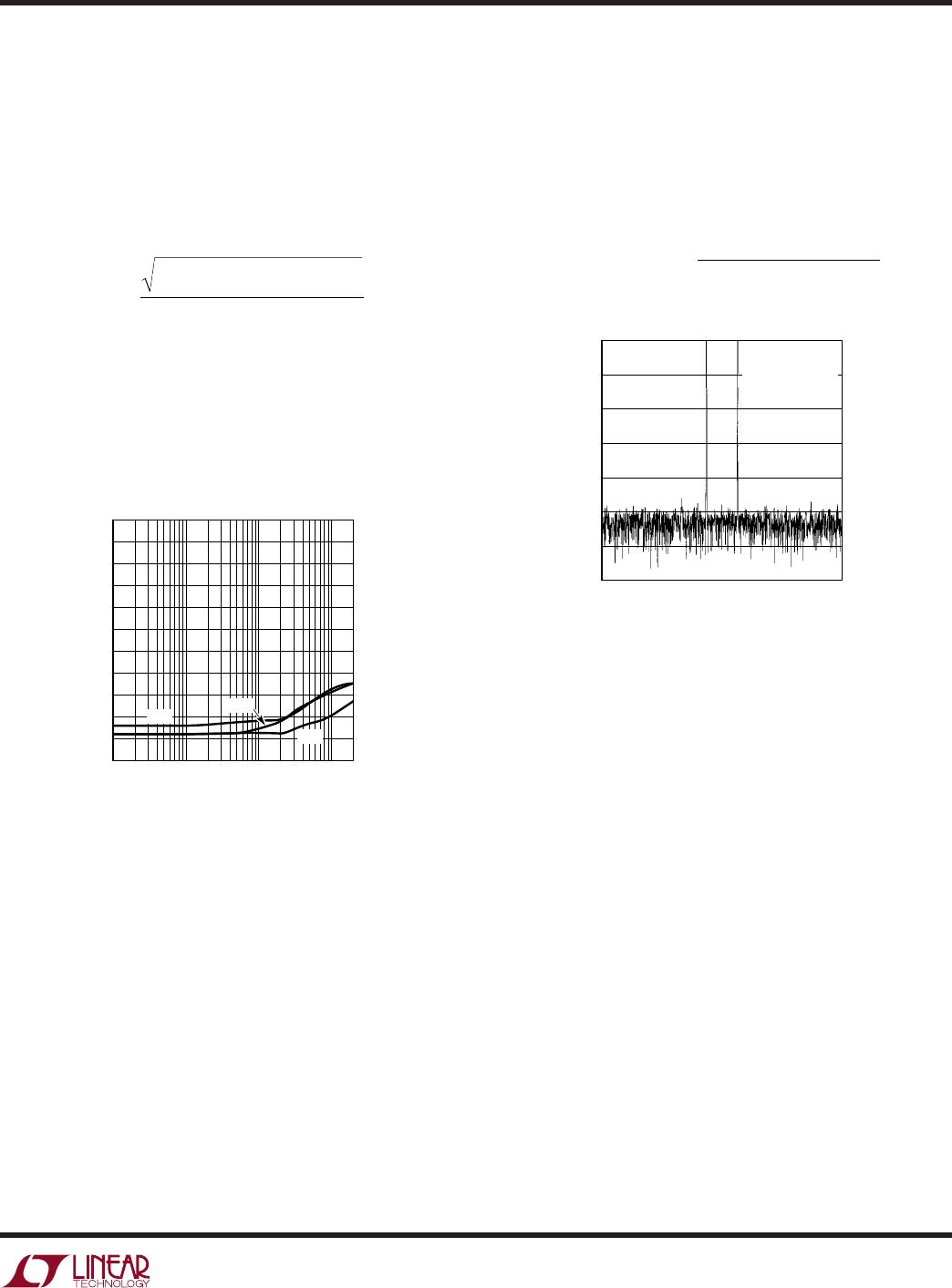
Figure 4. Distortion vs Input Frequency
Intermodulation Distortion
If the ADC input signal consists of more than one spectral
component, the ADC transfer function nonlinearity can
produce intermodulation distortion (IMD) in addition to
THD. IMD is the change in one sinusoidal input caused by
the presence of another sinusoidal input at a different
frequency.
If two pure sine waves of frequencies fa and fb are applied
to the ADC input, nonlinearities in the ADC transfer
function can create distortion products at the sum and
FREQUENCY (Hz)
0
AMPLITUDE (dB)
0
–20
–40
–60
–80
100
120
140
20
100
140
1416 G05
80
180
200
40
60
120 160
f
SAMPLE
= 400kHz
f
a
=87.01171876kHz
f
b
=113.1835938kHz
Figure 5. Intermodulation Distortion Plot
Peak Harmonic or Spurious Noise
The peak harmonic or spurious noise is the largest spec-
tral component excluding the input signal and DC. This
value is expressed in decibels relative to the RMS value of
a full-scale input signal.
Full-Power and Full-Linear Bandwidth
The full-power bandwidth is that input frequency at which
the amplitude of the reconstructed fundamental is
reduced by 3dB for a full-scale input signal. The full-linear
bandwidth is the input frequency at which the S/(N + D)
has dropped to 77dB (12.5 effective bits). The LTC1416
has been designed to optimize input bandwidth, allowing
the ADC to undersample input signals with frequencies
above the converter’s Nyquist frequency. The noise floor
stays very low at high frequencies; S/(N + D) becomes
dominated by distortion at frequencies far beyond Nyquist.

LTC1416CG#PBF

Mfr. #:
Manufacturer:
Analog Devices Inc.
Description:
Analog to Digital Converters - ADC 400ksps 14-Bit Parallel ADC
Lifecycle:
New from this manufacturer.
Delivery:
DHL FedEx Ups TNT EMS
Payment:
T/T Paypal Visa MoneyGram Western Union