LT3970 Series
13
3970fc
operation, the noise is typically very quiet to a casual ear.
If this is unacceptable, use a high performance tantalum
or electrolytic capacitor at the output.
A final precaution regarding ceramic capacitors concerns
the maximum input voltage rating of the LT3970. As pre
-
viously mentioned, a ceramic input capacitor combined
with trace or cable inductance forms a high quality (under
damped) tank circuit. If the L
T3970 circuit is plugged into a
live supply, the input voltage can ring to twice its nominal
value, possibly exceeding the LT3970’s rating. This situation
is easily avoided (see the Hot Plugging Safely section).
Low Ripple Burst Mode Operation
To enhance efficiency at light loads, the LT3970 operates
in low ripple Burst Mode operation which keeps the output
capacitor charged to the proper voltage while minimizing
the input quiescent current. During Burst Mode opera
-
tion, the LT3970 delivers single cycle bursts of current to
the output capacitor followed by sleep periods where the
output power is delivered to the load by the output capaci
-
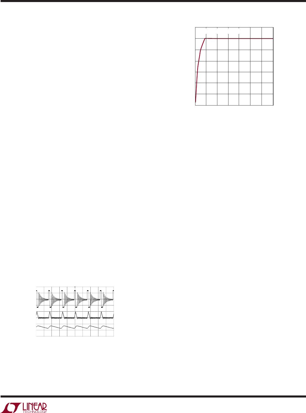
tor. Because the LT3970 delivers power to the output with
single, low current pulses, the output ripple is kept below
5mV for a typical application. See Figure 2.
As the load current decreases towards a no load condition,
the per
centage of time that the L
T3970 operates in sleep
mode increases and the average input current is greatly
reduced resulting in high efficiency even at very low loads.
Note that during Burst Mode operation, the switching
frequency will be lower than the programmed switching
frequency. See Figure 3.
At higher output loads (above ~45mA for the front page
application) the LT3970 will be running at the frequency
programmed by the R
T
resistor, and will be operating in
standard PWM mode. The transition between PWM and
low ripple Burst Mode is seamless, and will not disturb
the output voltage.
BOOST and BD Pin Considerations
Capacitor C3 and the internal boost Schottky diode (see the
Block Diagram) are used to generate a boost voltage that
is higher than the input voltage. In most cases a 0.22µF
capacitor will work well. Figure 4 shows two ways to ar
-
range the boost circuit. The BOOST pin must be more than
1.9V above the SW pin for best efficiency. For outputs of
2.2V and above, the standard circuit (Figure 4a) is best.
For outputs between 2.2V and 2.5V, use a 0.47µF boost
capacitor. For output voltages below 2.2V, the boost diode
can be tied to the input (Figure 4b), or to another external
supply greater than 2.2V. However, the circuit in Figure 4a
is more efficient because the BOOST pin current and BD
pin quiescent current come from a lower voltage source.
Also, be sure that the maximum voltage ratings of the
BOOST and BD pins are not exceeded.
The minimum operating voltage of an LT3970 application
is limited by the minimum input voltage (4.2V) and by the
maximum duty cycle as outlined in a previous section. For
output voltages greater than 3.4V, the minimum input volt
-
age is also limited by the boost circuit for proper start-up.
applicaTions inFormaTion
Figure 2. Burst Mode Operation
Figure 3. Switching Frequency in Burst Mode Operation
V
OUT
5mV/DIV
V
SW
5V/DIV
I
L
100mA/DIV
2µs/DIV
FRONT PAGE APPLICATION
V
IN
= 12V
V
OUT
= 5V
I
LOAD
= 10mA
3970 F02
LOAD CURRENT (mA)
0
400
500
700
150 250
3070 F03
300
200
50 100
200 300 350
100
0
600
SWITCHING FREQUENCY (kHz)
FRONT PAGE APPLICATION
LT3970 Series
14
3970fc
If the input voltage is ramped slowly, the boost capacitor
may not be fully charged. Because the boost capacitor is
charged with the energy stored in the inductor, the circuit
will rely on some minimum load current to get the boost
circuit running properly. This minimum load will depend
on input and output voltages, and on the arrangement of
the boost circuit. The minimum load generally goes to
zero once the circuit has started. Figure 5 shows a plot
of minimum load to start and to run as a function of input
voltage. In many cases the discharged output capacitor
will present a load to the switcher, which will allow it to
start. The plots show the worst-case situation where V
IN
is ramping very slowly. For lower start-up voltage, the
boost diode can be tied to V
IN
; however, this restricts the
input range to one-half of the absolute maximum rating
of the BOOST pin.
Enable Pin
The LT3970 is in shutdown when the EN pin is low and
active when the pin is high. The rising threshold of the EN
comparator is 1V, with a 30mV hysteresis. This threshold
is accurate when V
IN
is above 4.2V. If V
IN
is lower than
4.2V, tie EN pin to GND to place the part in shutdown.
applicaTions inFormaTion
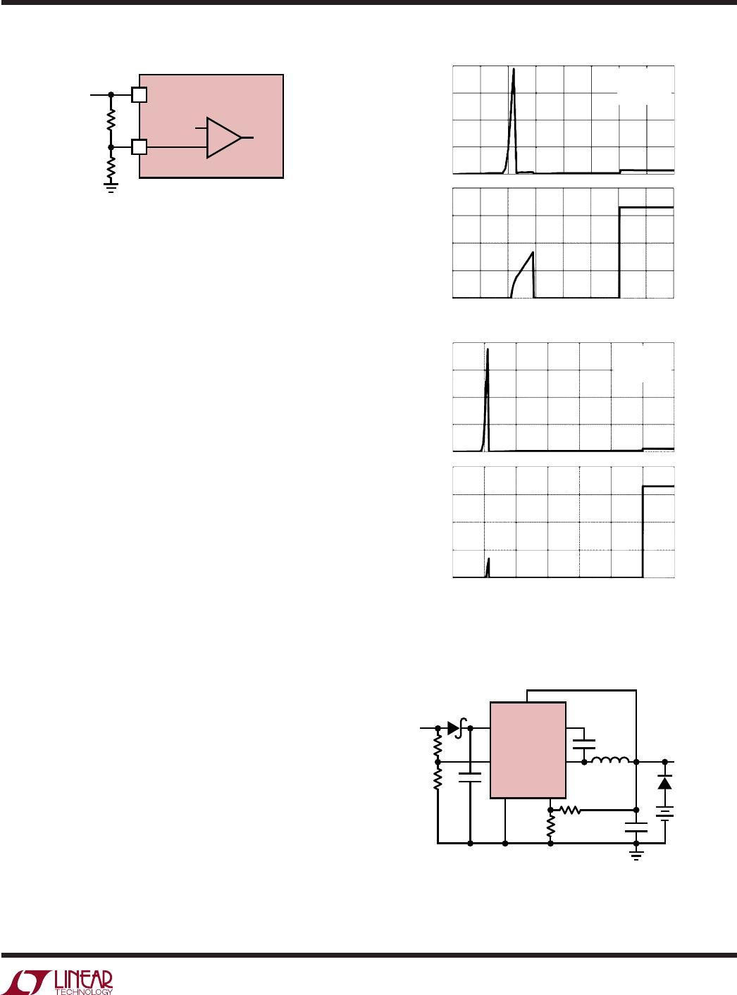
Figure 4. Two Circuits for Generating the Boost Voltage
Figure 5. The Minimum Input Voltage Depends on
Output Voltage, Load Current and Boost Circuit
Adding a resistor divider from V
IN
to EN programs the
LT3970 to regulate the output only when V
IN
is above a
desired voltage (see Figure 6). This threshold voltage,
V
IN(EN)
, can be adjusted by setting the values R3 and R4
such that they satisfy the following equation:
V
IN(EN)
=
R3+ R4
R4
1V
where output regulation should not start until V
IN
is above
V
IN(EN)
. Note that due to the comparators hysteresis,
regulation will not stop until the input falls slightly below
V
IN(EN)
.
BD
LT3970
(4a) For V
OUT
≥ 2.2V
BOOSTV
IN
V
IN
C3
V
OUT
SW
GND
BD
LT3970
(4b) For V
OUT
< 2.2V; V
IN
< 27V
BOOSTV
IN
V
IN
C3
3970 F04
V
OUT
SW
GND
LOAD CURRENT (mA)
0 50
2.5
INPUT VOLTAGE (V)
3.5
5.0
100
200
250
3.0
4.5
4.0
150
300
350
FRONT PAGE APPLICATION
V
OUT
= 3.3V
TO START/RUN
LOAD CURRENT (mA)
0 50
4.0
INPUT VOLTAGE (V)
5.0
6.5
100
200
250
3970 F05
4.5
6.0
5.5
150
300
350
FRONT PAGE APPLICATION
V
OUT
= 5V
TO START
TO RUN
LT3970 Series
15
3970fc
applicaTions inFormaTion
Be aware that while V
IN
is below 4.2V, the input current
may rise up to several hundred µA and the part may begin
to switch while the internal circuitry starts up. Figure 7
shows the startup behavior of a typical application with
different programmed V
IN(EN)
.
Shorted and Reversed Input Protection
If the inductor is chosen so that it won’t saturate exces
-
sively, a LT3970 buck regulator will tolerate a shorted
output. There is another situation to consider in systems
where the output will be held high when the input to the
LT3970 is absent. This may occur in battery charging ap
-
plications or in battery backup systems where a battery
or some other supply is diode ORed with the LT3970’
s
output. If the V
IN
pin is allowed to float and the EN pin
is held high (either by a logic signal or because it is tied
to V
IN
), then the LT3970’s internal circuitry will pull its
quiescent current through its SW pin. This is fine if the
system can tolerate a few µA in this state. If the EN pin is
grounded, the SW pin current will drop to 0.7µA. However,
if the V
IN
pin is grounded while the output is held high,
regardless of EN, parasitic diodes inside the LT3970 can
pull current from the output through the SW pin and the
V
IN
pin. Figure 8 shows a circuit that will run only when
the input voltage is present and that protects against a
shorted or reversed input.
Figure 8. Diode D4 Prevents a Shorted Input from Discharging a
Backup Battery Tied to the Output. It Also Protects the Circuit from
a Reversed Input. The LT3970 Runs Only when the Input is Present
160
120
INPUT CURRENT (µA)
80
40
0
4
INPUT VOLTAGE (V)
3
OUTPUT VOLTAGE (V)
2
1
0
160
120
INPUT CURRENT (µA)
80
40
0
4
3
OUTPUT VOLTAGE (V)
2
1
0
3970 F07
V
IN(EN)
= 6V
R3 = 5M
R4 = 1M
V
IN(EN)
= 12V
R3 = 11M
R4 = 1M
0 1 2 3 4 5 6 7 8
INPUT VOLTAGE (V)
0 2 4 6 8 10 12 14
Figure 7. V
IN
Start-Up of Front Page Application with V
OUT
= 3.3V,
No-Load Current, and V
IN(EN)
programmed as in Figure 6.
BD
LT3970
BOOSTV
IN
EN
V
IN
V
OUT
BACKUP
3970 F08
SW
D4
MBRS140
FBGND
+
Figure 6. Enable
+
1V
SHDN
3970 F06
LT3970
EN
V
IN
V
IN
R3
R4

LT3970EDDB-5#TRPBF

Mfr. #:
Manufacturer:
Analog Devices / Linear Technology
Description:
Switching Voltage Regulators 40V, 350mA Step-Down Regulator with 2uA Quiescent Current and Integrated Diodes
Lifecycle:
New from this manufacturer.
Delivery:
DHL FedEx Ups TNT EMS
Payment:
T/T Paypal Visa MoneyGram Western Union