LT3970 Series
19
3970fc
package DescripTion
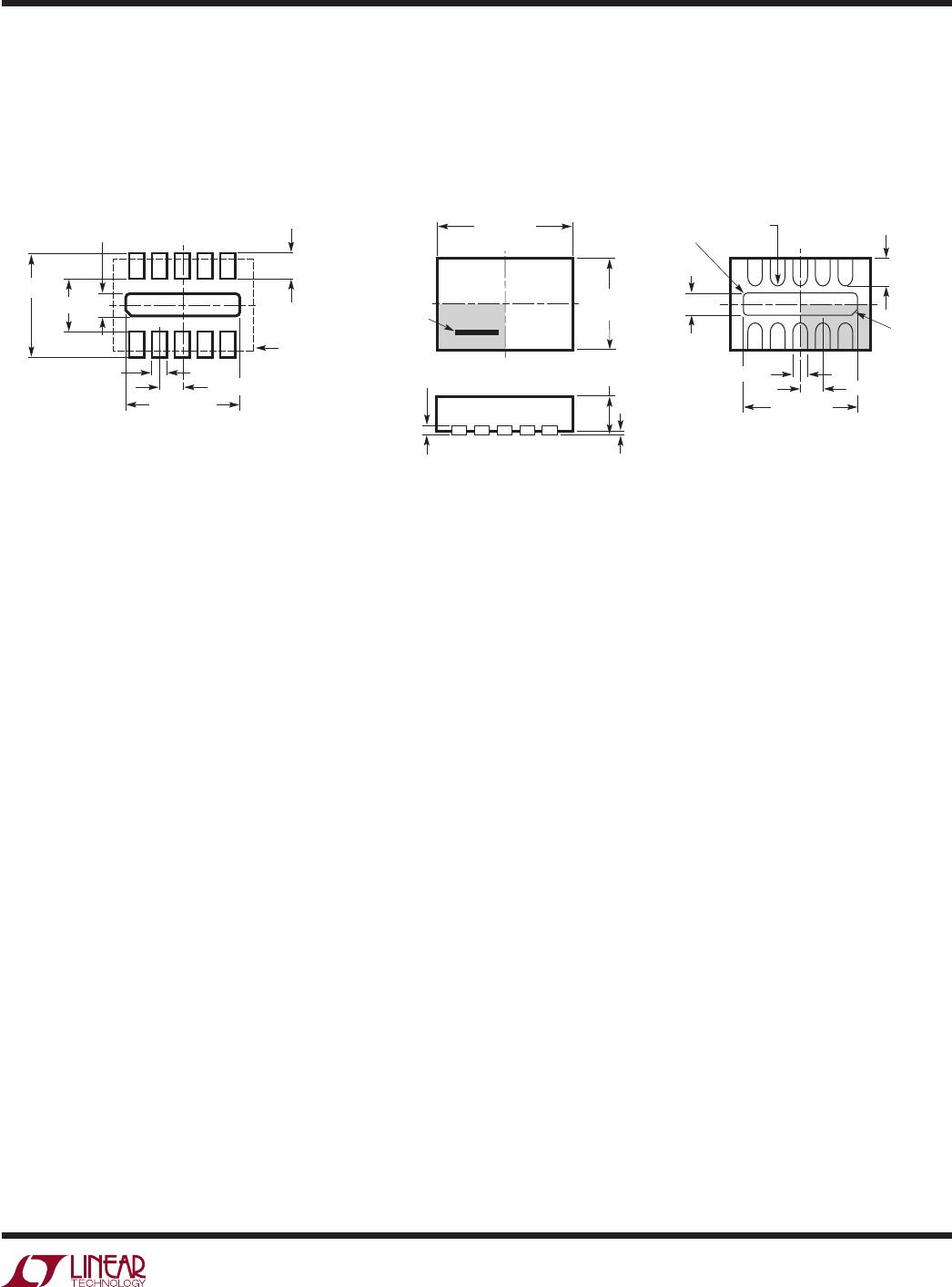
DDB Package
10-Lead Plastic DFN (3mm × 2mm)
(Reference LTC DWG # 05-08-1722 Rev Ø)
2.00 ±0.10
(2 SIDES)
NOTE:
1. DRAWING CONFORMS TO VERSION (WECD-1) IN JEDEC PACKAGE OUTLINE M0-229
2. DRAWING NOT TO SCALE
3. ALL DIMENSIONS ARE IN MILLIMETERS
4. DIMENSIONS OF EXPOSED PAD ON BOTTOM OF PACKAGE DO NOT INCLUDE
MOLD FLASH. MOLD FLASH, IF PRESENT, SHALL NOT EXCEED 0.15mm ON ANY SIDE
5. EXPOSED PAD SHALL BE SOLDER PLATED
6. SHADED AREA IS ONLY A REFERENCE FOR PIN 1 LOCATION ON THE TOP AND BOTTOM OF PACKAGE
0.40 ± 0.10
BOTTOM VIEW—EXPOSED PAD
0.64 ± 0.05
(2 SIDES)
0.75 ±0.05
R = 0.115
TYP
R = 0.05
TYP
2.39 ±0.05
(2 SIDES)
3.00 ±0.10
(2 SIDES)
15
106
PIN 1 BAR
TOP MARK
(SEE NOTE 6)
0.200 REF
0 – 0.05
(DDB10) DFN 0905 REV Ø
0.25 ± 0.05
2.39 ±0.05
(2 SIDES)
RECOMMENDED SOLDER PAD PITCH AND DIMENSIONS
0.64 ±0.05
(2 SIDES)
1.15 ±0.05
0.70 ±0.05
2.55 ±0.05
PACKAGE
OUTLINE
0.25 ± 0.05
0.50 BSC
PIN 1
R = 0.20 OR
0.25 × 45°
CHAMFER
0.50 BSC
Please refer to http://www.linear.com/designtools/packaging/ for the most recent package drawings.
LT3970 Series
20
3970fc
package DescripTion
MSOP (MS) 0307 REV E
0.53 ± 0.152
(.021 ± .006)
SEATING
PLANE
0.18
(.007)
1.10
(.043)
MAX
0.17 –0.27
(.007 – .011)
TYP
0.86
(.034)
REF
0.50
(.0197)
BSC
1 2
3
4 5
4.90 ± 0.152
(.193 ± .006)
0.497 ± 0.076
(.0196 ± .003)
REF
8910
7
6
3.00 ± 0.102
(.118 ± .004)
(NOTE 3)
3.00 ± 0.102
(.118 ± .004)
(NOTE 4)
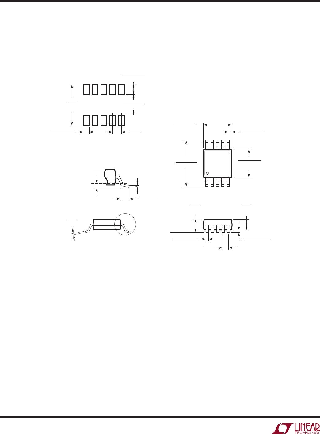
NOTE:
1. DIMENSIONS IN MILLIMETER/(INCH)
2. DRAWING NOT TO SCALE
3. DIMENSION DOES NOT INCLUDE MOLD FLASH, PROTRUSIONS OR GATE BURRS.
MOLD FLASH, PROTRUSIONS OR GATE BURRS SHALL NOT EXCEED 0.152mm (.006") PER SIDE
4. DIMENSION DOES NOT INCLUDE INTERLEAD FLASH OR PROTRUSIONS.
INTERLEAD FLASH OR PROTRUSIONS SHALL NOT EXCEED 0.152mm (.006") PER SIDE
5. LEAD COPLANARITY (BOTTOM OF LEADS AFTER FORMING) SHALL BE 0.102mm (.004") MAX
0.254
(.010)
0° – 6° TYP
DETAIL “A”
DETAIL “A”
GAUGE PLANE
5.23
(.206)
MIN
3.20 – 3.45
(.126 – .136)
0.889 ± 0.127
(.035 ± .005)
RECOMMENDED SOLDER PAD LAYOUT
0.305 ± 0.038
(.0120 ± .0015)
TYP
0.50
(.0197)
BSC
0.1016 ± 0.0508
(.004 ± .002)
MS Package
10-Lead Plastic MSOP
(Reference LTC DWG # 05-08-1661 Rev E)
Please refer to http://www.linear.com/designtools/packaging/ for the most recent package drawings.
LT3970 Series
21
3970fc
Information furnished by Linear Technology Corporation is believed to be accurate and reliable.
However, no responsibility is assumed for its use. Linear Technology Corporation makes no representa-
tion that the interconnection of its circuits as described herein will not infringe on existing patent rights.
revision hisTory
REV DATE DESCRIPTION PAGE NUMBER
A 5/10 Added LT3970-3.3 and LT3970-5 1 - 22
B 3/12 Title and Features clarified to add 3.42V fixed output version.
Clarified the Absolute Maximum Ratings section, added 3.42V output option in the Order Information section.
Added 3.42V output option in the Electrical Characteristics table.
Added 3.42V Output Voltage vs Temperature graph.
Clarified V
OUT
Pin Function and Block Diagram.
1
2
3
4
8
C 09/13 Added H-grade MSOP-10E version to Order Information table
Clarified Feedback Voltage Specifications to 150°C
2
3
LT3970EDDB-5#TRPBF

Mfr. #:
Manufacturer:
Analog Devices / Linear Technology
Description:
Switching Voltage Regulators 40V, 350mA Step-Down Regulator with 2uA Quiescent Current and Integrated Diodes
Lifecycle:
New from this manufacturer.
Delivery:
DHL FedEx Ups TNT EMS
Payment:
T/T Paypal Visa MoneyGram Western Union