LT3970 Series
16
3970fc
applicaTions inFormaTion
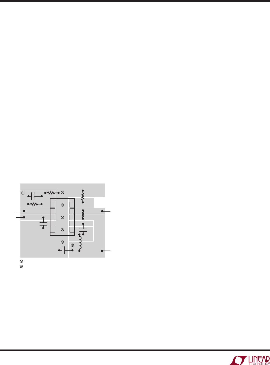
PCB Layout
For proper operation and minimum EMI, care must be
taken during printed circuit board layout. Figure 9 shows
the recommended component placement with trace,
ground plane and via locations. Note that large, switched
currents flow in the LT3970’s V
IN
and SW pins, the internal
catch diode and the input capacitor. The loop formed by
these components should be as small as possible. These
components, along with the inductor and output capacitor,
should be placed on the same side of the circuit board,
and their connections should be made on that layer. Place
a local, unbroken ground plane below these components.
The SW and BOOST nodes should be as small as possible.
Finally, keep the FB nodes small so that the ground traces
will shield them from the SW and BOOST nodes. The
Exposed Pad on the bottom of the DFN package must be
soldered to ground so that the pad acts as a heat sink. To
keep thermal resistance low, extend the ground plane as
much as possible, and add thermal vias under and near
the LT3970 to additional ground planes within the circuit
board and on the bottom side.
Figure 9. A Good PCB Layout Ensures Proper, Low EMI Operation
with stray inductance in series with the power source,
forms an under damped tank circuit, and the voltage at
the V
IN
pin of the LT3970 can ring to twice the nominal
input voltage, possibly exceeding the LT3970’s rating and
damaging the part. If the input supply is poorly controlled
or the user will be plugging the LT3970 into an energized
supply, the input network should be designed to prevent
this overshoot. See Linear Technology Application Note 88
for a complete discussion.
High Temperature Considerations
For higher ambient temperatures, care should be taken
in the layout of the PCB to ensure good heat sinking
of the LT3970. The Exposed Pad on the bottom of the
DFN package must be soldered to a ground plane. This
ground should be tied to large copper layers below with
thermal vias; these layers will spread the heat dissipated
by the LT3970. Placing additional vias can reduce thermal
resistance further. In the MSOP package, the copper lead
frame is fused to GND (Pin 5) so place thermal vias near
this pin. The maximum load current should be derated
as the ambient temperature approaches the maximum
junction rating.
Power dissipation within the LT3970 can be estimated by
calculating the total power loss from an efficiency measure
-
ment and subtracting inductor loss. The die temperature
is calculated by multiplying the LT3970 power dissipation
by the thermal resistance from junction to ambient.
Finally
, be aware that at high ambient temperatures the
internal Schottky diode will have significant leakage current
(see Typical Performance Characteristics) increasing the
quiescent current of the LT3970 converter.
Other Linear Technology Publications
Application Notes 19, 35 and 44 contain more detailed
descriptions and design information for buck regulators
and other switching regulators. The LT1376 data sheet
has a more extensive discussion of output ripple, loop
compensation and stability testing. Design Note 100
shows how to generate a bipolar output supply using a
buck regulator.
6
8
7
9
10
5
4
2
3
1
VIAS TO LOCAL GROUND PLANE
VIAS TO V
EN
GND
GND
PG
V
OUT
GND
V
IN
3970 F09
Hot Plugging Safely
The small size, robustness and low impedance of ceramic
capacitors make them an attractive option for the input
bypass capacitor of LT3970 circuits. However, these ca
-
pacitors can cause problems if the LT3970 is plugged into
a live supply. The low loss ceramic capacitor
, combined

