IDT70V659/58/57S
High-Speed 3.3V 128/64/32K x 36 Asynchronous Dual-Port Static RAM Industrial and Commercial Temperature Ranges
16
Timing Waveform of Write with Port-to-Port Read and BUSY (M/S = VIH)
(2,4,5)
Timing Waveform of Write with BUSY (M/S = VIL)
NOTES:
1. t
WH must be met for both BUSY input (SLAVE) and output (MASTER).
2. BUSY is asserted on port "B" blocking R/W
"B", until BUSY"B" goes HIGH.
3. t
WB is only for the 'slave' version.
NOTES:
1. To ensure that the earlier of the two ports wins. t
APS is ignored for M/S = VIL (SLAVE).
2. CE
L = CER = VIL.
3. OE = V
IL for the reading port.
4. If M/S = V
IL (slave), BUSY is an input. Then for this example BUSY"A" = VIH and BUSY"B" input is shown above.
5. All timing is the same for left and right ports. Port "A" may be either the left or right port. Port "B" is the port opposite from port "A".
4869 drw 12
t
DW
t
APS
ADDR
"A"
t
WC
DATA
OUT "B"
MATCH
t
WP
R/W
"A"
DATA
IN "A"
ADDR
"B"
t
DH
VALID
(1)
MATCH
BUSY
"B"
t
BDA
VALID
t
BDD
t
DDD
(3)
t
WDD
t
BAA
.
4869 drw 13
R/W
"A"
BUSY
"B"
t
WB
(3)
R/W
"B"
t
WH
(1)
(2)
t
WP
.
17
IDT70V659/58/57S
High-Speed 3.3V 128/64/32K x 36 Asynchronous Dual-Port Static RAM Industrial and Commercial Temperature Ranges
AC Electrical Characteristics Over the
Operating Temperature and Supply Voltage Range
Waveform of BUSY Arbitration Controlled by CE Timing
(M/S = VIH)
(1)
Waveform of BUSY Arbitration Cycle Controlled by Address Match
Timing
(M/S = VIH)
(1)
NOTES:
1. All timing is the same for left and right ports. Port “A” may be either the left or right port. Port “B” is the port opposite from port “A”.
2. If t
APS is not satisfied, the BUSY signal will be asserted on one side or another but there is no guarantee on which side BUSY will be asserted.
4869 drw 1
4
ADDR
"A"
and
"B"
ADDRESSES MATCH
CE
"A"
CE
"B"
BUSY
"B"
t
APS
t
BAC
t
BDC
(2)
4869 drw 1
5
ADDR
"A"
ADDRESS "N"
ADDR
"B"
BUSY
"B"
t
APS
t
BAA
t
BDA
(2)
MATCHING ADDRESS "N"
,
70V659/58/57S10
Com'l Only
70V659/58/57S12
Com'l
& Ind
70V659/58/57S15
Com'l
& Ind
Symbol Parameter Min.Max.Min.Max.Min.Max.Unit
INTERRUPT TIMING
t
AS
Address Set-up Time 0
____
0
____
0
____
ns
t
WR
Write Recovery Time 0
____
0
____
0
____
ns
t
INS
Interrupt Set Time
____
10
____
12
____
15 ns
t
INR
Interrupt Reset Time
____
10
____
12
____
15 ns
4869 tbl 15
IDT70V659/58/57S
High-Speed 3.3V 128/64/32K x 36 Asynchronous Dual-Port Static RAM Industrial and Commercial Temperature Ranges
18
Truth Table III — Interrupt Flag
(1,4)
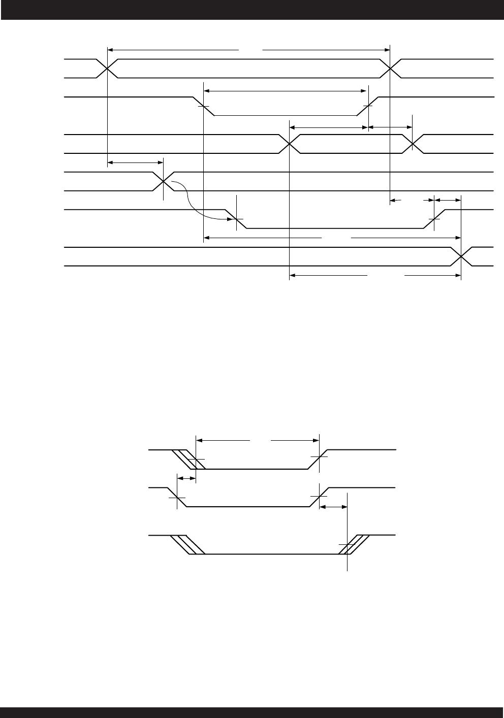
Waveform of Interrupt Timing
(1)
NOTES:
1. All timing is the same for left and right ports. Port “A” may be either the left or right port. Port “B” is the port opposite from port “A”.
2. Refer to Interrupt Truth Table.
3. Timing depends on which enable signal (CE or R/W) is asserted last.
4. Timing depends on which enable signal (CE
or R/W) is de-asserted first.
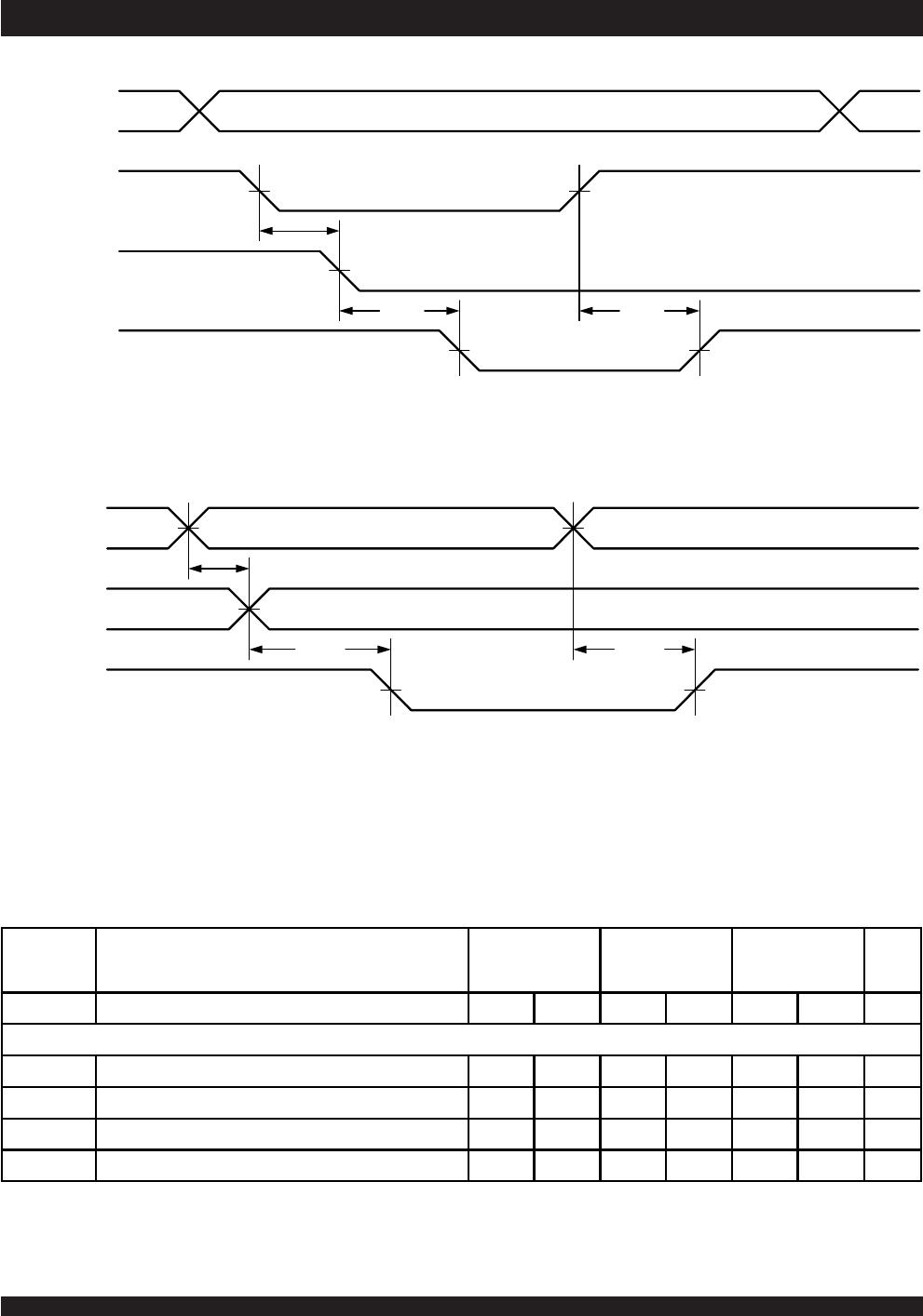
NOTES:
1. Assumes BUSY
L = BUSYR =VIH.
2. If BUSY
L = VIL, then no change.
3. If BUSY
R = VIL, then no change.
4. INT
L and INTR must be initialized at power-up.
5. A
16x is a NC for IDT70V658, therefore Interrupt Addresses are FFFF and FFFE.
6. A
16x and A15x are NC's for IDT70V657, therefore Interrupt Addresses are 7FFF and 7FFE.
4869 drw 16
ADDR
"A"
INTERRUPT SET ADDRESS
CE
"A"
R/W
"A"
t
AS
t
WC
t
WR
(3)
(4)
t
INS
(3)
INT
"B"
(2)
4869 drw 17
ADDR
"B"
INTERRUPT CLEAR ADDRESS
CE
"B"
OE
"B"
t
AS
t
RC
(3)
t
INR
(3)
INT
"B"
(2)
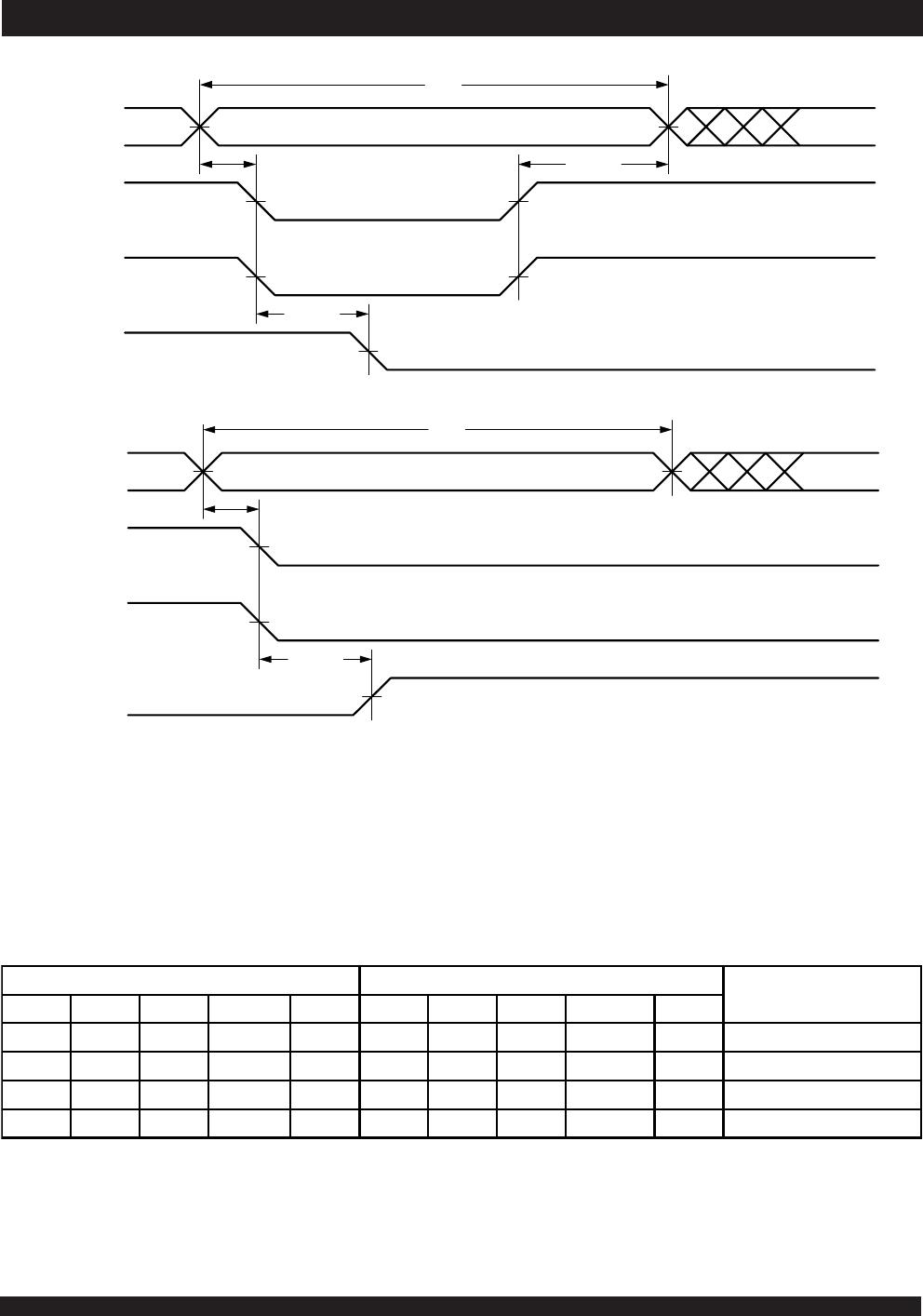
Left Port Right Port
FunctionR/W
L
CE
L
OE
L
A
16L
-A
0L
(5,6)
INT
L
R/W
R
CE
R
OE
R
A
16R
-A
0R
(5,6)
INT
R
L L X 1FFFF XXXX X L
(2 )
Set Right INT
R
Flag
XXXXXXLL1FFFFH
(3 )
Reset Right INT
R
Flag
XXX X L
(3 )
L L X 1FFFE X Set Left INT
L
Flag
X L L 1FFFE H
(2 )
X X X X X Reset Left INT
L
Flag
4869 tbl 16

70V658S15BC8

Mfr. #:
Manufacturer:
IDT
Description:
SRAM 64Kx36 STD-PWR, 3.3V DUAL-PORT RAM
Lifecycle:
New from this manufacturer.
Delivery:
DHL FedEx Ups TNT EMS
Payment:
T/T Paypal Visa MoneyGram Western Union