IDT70V659/58/57S
High-Speed 3.3V 128/64/32K x 36 Asynchronous Dual-Port Static RAM Industrial and Commercial Temperature Ranges
22
JTAG AC Electrical
Characteristics
(1,2,3,4)
Symbol Parameter Min. Max. Units
t
JCYC
JTAG Clock Input Period 100
____
ns
t
JCH
JTAG Clock HIGH 40
____
ns
t
JCL
JTAG Clock Low 40
____
ns
t
JR
JTAG Clock Rise Time
____
3
(1)
ns
t
JF
JTAG Clock Fall Time
____
3
(1)
ns
t
JRST
JTAG Reset 50
____
ns
t
JRSR
JTAG Reset Recovery 50
____
ns
t
JCD
JTAG Data Output
____
25 ns
t
JDC
JTAG Data Output Hold 0
____
ns
t
JS
JTAG Setup 15
____
ns
t
JH
JTAG Hold 15
____
ns
4869 tbl 19
NOTES:
1. Guaranteed by design.
2. 30pF loading on external output signals.
3. Refer to AC Electrical Test Conditions stated earlier in this document.
4. JTAG operations occur at one speed (10MHz). The base device may run at
any speed specified in this datasheet.
JTAG Timing Specifications
TCK
Device Inputs
(1)
/
TDI/TMS
D
evice Outputs
(2)
/
TDO
TRST
t
JCD
t
JDC
t
JRST
t
JS
t
JH
t
JCYC
t
JRSR
t
JF
t
JCL
t
JR
t
JCH
4869 drw 20
x
NOTES:
1. Device inputs = All device inputs except TDI, TMS, and TRST.
2. Device outputs = All device outputs except TDO.
23
IDT70V659/58/57S
High-Speed 3.3V 128/64/32K x 36 Asynchronous Dual-Port Static RAM Industrial and Commercial Temperature Ranges
Identification Register Definitions
Instruction Field Value Description
Revision Number (31:28) 0x0 Reserved for version number
IDT Device ID (27:12)
0x303
(1)
Defines IDT part number
IDT JEDEC ID (11:1) 0x33 Allows unique identification of device vendor as IDT
ID Register Indicator Bit (Bit 0) 1 Indicates the presence of an ID register
4869 tbl 20
Scan Register Sizes
Register Name Bit Size
Instruction (IR) 4
Bypass (BYR) 1
Identification (IDR) 32
Boundary Scan (BSR) Note (3)
4869 tbl 21
System Interface Parameters
Instruction Code Description
EXTEST 0000 Forces contents of the boundary scan cells onto the device outputs
(1)
.
Places the boundary scan register (BSR) between TDI and TDO.
BYPASS 1111 Places the bypass register (BYR) between TDI and TDO.
IDCODE 0010 Loads the ID register (IDR) with the vendor ID code and places the
register between TDI and TDO.
HIGHZ
0100 Places the bypass register (BYR) between TDI and TDO. Forces all
device output drivers to a High-Z state.
CLAMP 0011
Uses BYR. Forces contents of the boundary scan cells onto the device
outputs. Places the bypass register (BYR) between TDI and TDO.
SAMPLE/PRELOAD 0001 Places the boundary scan register (BSR) between TDI and TDO.
SAMPLE allows data from device inputs
(2 )
and outputs
(1 )
to be captured
in the boundary scan cells and shifted serially through TDO. PRELOAD
allows data to be input serially into the boundary scan cells via the TDI.
RESERVED All other codes Several combinations are reserved. Do not use codes other than those
identified above.
4869 tbl 22
NOTES:
1. Device outputs = All device outputs except TDO.
2. Device inputs = All device inputs except TDI, TMS, and TRST.
3. The Boundary Scan Descriptive Language (BSDL) file for this device is available on the IDT website (www.idt.com), or by contacting your local
IDT sales representative.
NOTE:
1. Device ID for IDT70V658 is 0x30B. Device ID for IDT70V657 is 0x323.
IDT70V659/58/57S
High-Speed 3.3V 128/64/32K x 36 Asynchronous Dual-Port Static RAM Industrial and Commercial Temperature Ranges
24
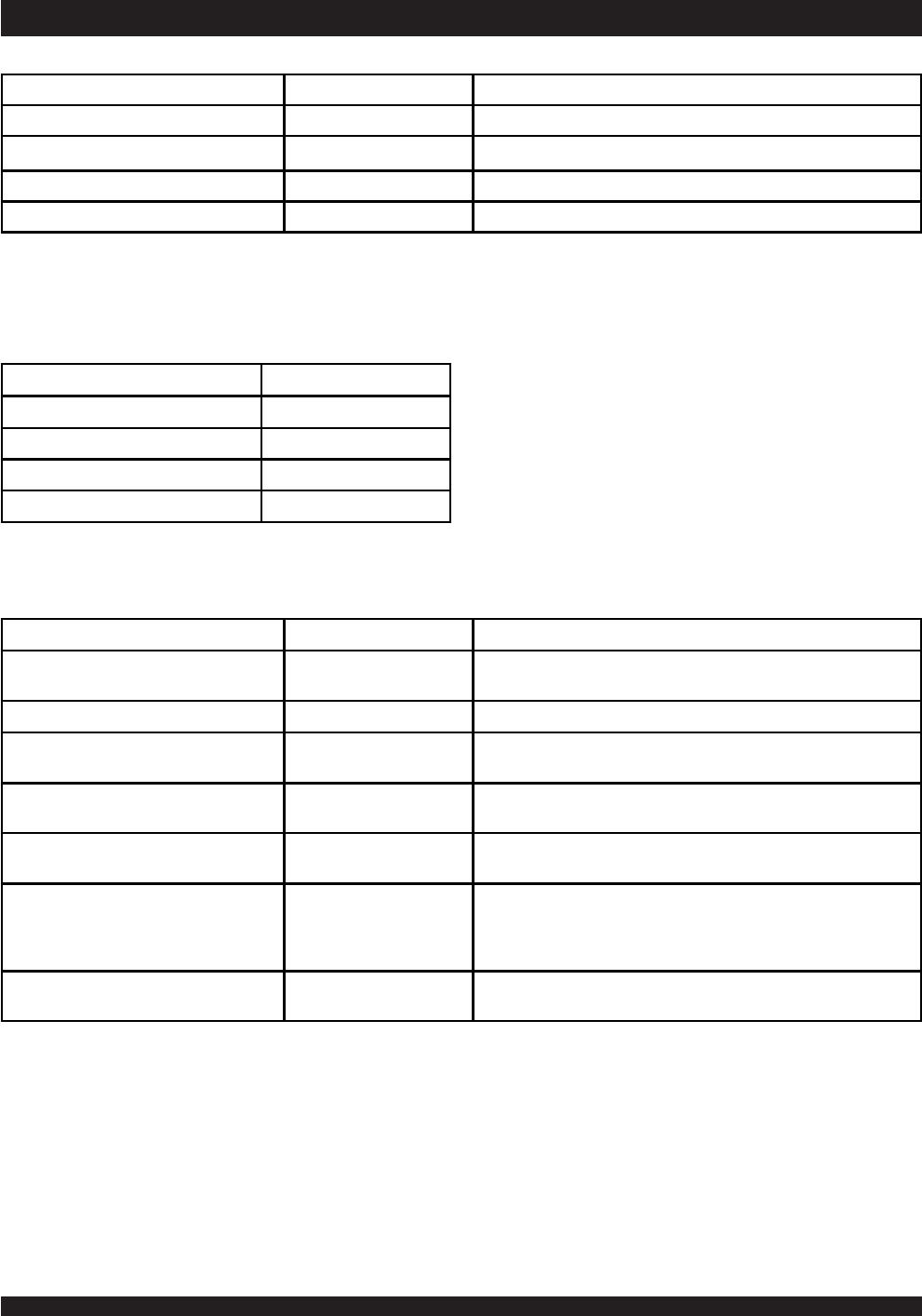
Ordering Information
4869 drw 21
Commercial (0°Cto+70°C)
Industrial (-40°Cto+85°C)
208-ball fpBGA (BF-208)
208-pin PQFP (DR-208)
256-ball BGA (BC-256)
Standard Power
Speed in nanoseconds
Commercial Only
Commercial & Industrial
4Mbit (128K x 36) 3.3V Asynchronous Dual-Port RAM
2Mbit (64K x 36) 3.3V Asynchronous Dual-Port RAM
1Mbit (32K x 36) 3.3V Asynchronous Dual-Port RAM
A
Power
999
Speed
A
Package
A
Process/
Temperature
Range
Blank
I
(1)
BF
DR
BC
10
12
15
S
70V659
70V658
70V657
XXXXX
Device
Type
A
G
(2)
Green
The IDT logo is a registered trademark of Integrated Device Technology, Inc.
Datasheet Document History:
6/2/00: Initial Public Offering
8/11/00: Page 6, 13 & 20 Inserted additional BEn information
6/20/01: Page 14 Increased BUSY TIMING parameters tBDA, tBAC, tBDC and tBDD for all speeds
Page 21 Changed maximum value for JTAG AC Electrical Characteristics for tJCD from 20ns to 25ns
12/17/01: Page 2, 3 & 4 Added date revision for pin configurations
Page 8, 10, 14 & 16 Removed I-temp 15ns speed from DC & AC Electrical Characteristics
Page 23 Removed I-temp 15ns speed from ordering information
Added I-temp footnote
Page 1 & 23 Replaced TM logo with ® logo
03/19/04: Consolidated multiple devices into one data sheet
Removed "Preliminary" Status
03/22/05: Page 1 Added green availability to features
Page 24 Added green indicator to ordering information
Page 1 & 24 Replaced old IDT TM with new IDT TM logo
07/25/08: Page 9 Corrected a typo in the DC Chars table
10/23/08: Page 24 Removed "IDT" from orderable part number
CORPORATE HEADQUARTERS for SALES: for Tech Support:
6024 Silver Creek Valley Road 800-345-7015 or 408-284-8200 408-284-2794
San Jose, CA 95138 fax: 408-284-2775 DualPortHelp@idt.com
www.idt.com
Notes:
1. Contact your local sales office for Industrial temp range in other speeds, packages and powers.
2. Green parts available. For specific speeds, packages and powers contact your local sales office.

70V658S15BC8

Mfr. #:
Manufacturer:
IDT
Description:
SRAM 64Kx36 STD-PWR, 3.3V DUAL-PORT RAM
Lifecycle:
New from this manufacturer.
Delivery:
DHL FedEx Ups TNT EMS
Payment:
T/T Paypal Visa MoneyGram Western Union