19
IDT70V659/58/57S
High-Speed 3.3V 128/64/32K x 36 Asynchronous Dual-Port Static RAM Industrial and Commercial Temperature Ranges
Functional Description
The IDT70V659/58/57 provides two ports with separate control,
address and I/O pins that permit independent access for reads or writes
to any location in memory. The IDT70V659/58/57 has an automatic power
down feature controlled by CE. The CE0 and CE1 control the on-chip
power down circuitry that permits the respective port to go into a standby
mode when not selected (CE = HIGH). When a port is enabled, access
to the entire memory array is permitted.
Interrupts
If the user chooses the interrupt function, a memory location (mail box
or message center) is assigned to each port. The left port interrupt flag
(INTL) is asserted when the right port writes to memory location 1FFFE
(HEX) (FFFE for IDT70V658 and 7FFE for IDT70V657), where a write
is defined as CER = R/WR = VIL per the Truth Table III. The left port clears
the interrupt through access of address location 1FFFE (FFFE for
IDT70V658 and 7FFE for IDT70V657) when CEL = OEL = VIL, R/W is
Truth Table IV —
Address BUSY Arbitration
NOTES:
1. Pins BUSY
L and BUSYR are both outputs when the part is configured as a master. Both are inputs when configured as a slave. BUSY outputs on the
IDT70V659/58/57 are push-pull, not open drain outputs. On slaves the BUSY
input internally inhibits writes.
2. "L" if the inputs to the opposite port were stable prior to the address and enable inputs of this port. "H" if the inputs to the opposite port became stable after the address
and enable inputs of this port. If t
APS is not met, either BUSYL or BUSYR = LOW will result. BUSYL and BUSYR outputs can not be LOW simultaneously.
3. Writes to the left port are internally ignored when BUSY
L outputs are driving LOW regardless of actual logic level on the pin. Writes to the right port are internally ignored
when BUSY
R outputs are driving LOW regardless of actual logic level on the pin.
4. A
16X is a NC for IDT70V658, therefore Address comparison will be for A0 - A15. Also, A16X and A15X are NC's for IDT70V657, therefore Address comparison will
be for A
0 - A14.
Inputs Outputs
Function
CE
L
CE
R
A
OL
-A
16L
(4)
A
OR
-A
16R
BUSY
L
(1)
BUSY
R
(1)
X X NO MATCH H H Normal
HXMATCHHHNormal
XHMATCHH HNormal
LL MATCH (2) (2)
Write Inhibit
(3)
4869 tbl 17
Truth Table V — Example of Semaphore Procurement Sequence
(1,2,3)
NOTES:
1. This table denotes a sequence of events for only one of the eight semaphores on the IDT70V659/58/57.
2. There are eight semaphore flags written to via I/O
0 and read from all I/O's (I/O0-I/O35). These eight semaphores are addressed by A0 - A2.
3. CE = V
IH, SEM = VIL to access the semaphores. Refer to the Semaphore Read/Write Control Truth Table.
Functions D
0
- D
35
Left D
0
- D
35
Right Status
No Action 1 1 Semaphore free
Left Port Writes "0" to Semaphore 0 1 Left port has semaphore token
Right Port Writes "0" to Semaphore 0 1 No change. Right side has no write access to semaphore
Left Port Writes "1" to Semaphore 1 0 Right port obtains semaphore token
Left Port Writes "0" to Semaphore 1 0 No change. Left port has no write access to semaphore
Right Port Writes "1" to Semaphore 0 1 Left port obtains semaphore token
Left Port Writes "1" to Semaphore 1 1 Semaphore free
Right Port Writes "0" to Semaphore 1 0 Right port has semaphore token
Right Port Writes "1" to Semaphore 1 1 Semaphore free
Left Port Writes "0" to Semaphore 0 1 Left port has semaphore token
Left Port Writes "1" to Semaphore 1 1 Semaphore free
4869 tbl 18
IDT70V659/58/57S
High-Speed 3.3V 128/64/32K x 36 Asynchronous Dual-Port Static RAM Industrial and Commercial Temperature Ranges
20
Busy Logic
Busy Logic provides a hardware indication that both ports of the RAM
have accessed the same location at the same time. It also allows one of the
two accesses to proceed and signals the other side that the RAM is “Busy”.
The BUSY pin can then be used to stall the access until the operation on
the other side is completed. If a write operation has been attempted from
the side that receives a BUSY indication, the write signal is gated internally
to prevent the write from proceeding.
The use of BUSY logic is not required or desirable for all applications.
In some cases it may be useful to logically OR the BUSY outputs together
and use any BUSY indication as an interrupt source to flag the event of
an illegal or illogical operation. If the write inhibit function of BUSY logic is
not desirable, the BUSY logic can be disabled by placing the part in slave
mode with the M/S pin. Once in slave mode the BUSY pin operates solely
as a write inhibit input pin. Normal operation can be programmed by tying
the BUSY pins HIGH. If desired, unintended write operations can be
prevented to a port by tying the BUSY pin for that port LOW.
The BUSY outputs on the IDT70V659/58/57 RAM in master mode,
are push-pull type outputs and do not require pull up resistors to operate.
If these RAMs are being expanded in depth, then the BUSY indication
for the resulting array requires the use of an external AND gate.
If two or more master parts were used when expanding in width, a split
decision could result with one master indicating BUSY on one side of the
array and another master indicating BUSY on one other side of
the array. This would inhibit the write operations from one port for part of
a word and inhibit the write operations from the other port for the other part
of the word.
The BUSY arbitration on a master is based on the chip enable and
address signals only. It ignores whether an access is a read or write. In
a master/slave array, both address and chip enable must be valid long
enough for a BUSY flag to be output from the master before the actual write
pulse can be initiated with the R/W signal. Failure to observe this timing
can result in a glitched internal write inhibit signal and corrupted data in the
slave.
Semaphores
The IDT70V659/58/57 is an extremely fast Dual-Port 128/64/32K x
36 CMOS Static RAM with an additional 8 address locations dedicated to
binary semaphore flags. These flags allow either processor on the left or
right side of the Dual-Port RAM to claim a privilege over the other processor
for functions defined by the system designer’s software. As an example,
the semaphore can be used by one processor to inhibit the other from
accessing a portion of the Dual-Port RAM or any other shared resource.
The Dual-Port RAM features a fast access time, with both ports being
completely independent of each other. This means that the activity on the
left port in no way slows the access time of the right port. Both ports are
identical in function to standard CMOS Static RAM and can be read from
or written to at the same time with the only possible conflict arising from the
simultaneous writing of, or a simultaneous READ/WRITE of, a non-
semaphore location. Semaphores are protected against such ambiguous
situations and may be used by the system program to avoid any conflicts
in the non-semaphore portion of the Dual-Port RAM. These devices have
an automatic power-down feature controlled by CE, the Dual-Port RAM
enable, and SEM, the semaphore enable. The CE and SEM pins control
on-chip power down circuitry that permits the respective port to go into
standby mode when not selected.
Systems which can best use the IDT70V659/58/57 contain multiple
processors or controllers and are typically very high-speed systems
which are software controlled or software intensive. These systems
can benefit from a performance increase offered by the IDT70V659/58/
57s hardware semaphores, which provide a lockout mechanism without
requiring complex programming.
Software handshaking between processors offers the maximum in
system flexibility by permitting shared resources to be allocated in varying
configurations. The IDT70V659/58/57 does not use its semaphore
flags to control any resources through hardware, thus allowing the system
designer total flexibility in system architecture.
An advantage of using semaphores rather than the more common
methods of hardware arbitration is that wait states are never incurred in
either processor. This can prove to be a major advantage in very high-
speed systems.
4869 drw 18
MASTER
Dual Port RAM
BUSY
R
CE
0
MASTER
Dual Port RAM
BUSY
R
SLAVE
Dual Port RAM
BUSY
R
SLAVE
Dual Port RAM
BUSY
R
CE
1
CE
1
CE
0
A
17
(1,2)
BUSY
L
BUSY
L
BUSY
L
BUSY
L
.
a "don't care". Likewise, the right port interrupt flag (INTR) is asserted when
the left port writes to memory location 1FFFF (HEX) (FFFF for IDT70V658
and 7FFF for IDT70V657) and to clear the interrupt flag (INT
R), the right
port must read the memory location 1FFFF (FFFF for IDT70V658 and
7FFF for IDT70V657). The message (36 bits) at 1FFFE (FFFE for
IDT70V658 and 7FFE for IDT70V657)or 1FFFF (FFFF for IDT70V658
and 7FFF for IDT70V657) is user-defined since it is an addressable
SRAM location. If the interrupt function is not used, address locations
1FFFE (FFFE for IDT70V658 and 7FFE for IDT70V657) and 1FFFF
(FFFF for IDT70V658 and 7FFF for IDT70V657) are not used as mail
boxes, but as part of the random access memory. Refer to Truth Table III
for the interrupt operation.
Width Expansion with Busy Logic
Master/Slave Arrays
When expanding an IDT70V659/58/57 RAM array in width while
using BUSY logic, one master part is used to decide which side of the RAMs
array will receive a BUSY indication, and to output that indication. Any
Figure 3. Busy and chip enable routing for both width and depth
expansion with IDT70V659/58/57 RAMs.
number of slaves to be addressed in the same address range as the master
use the BUSY signal as a write inhibit signal. Thus on the IDT70V659/58/
57 RAM the BUSY pin is an output if the part is used as a master (M/S pin
= V
IH), and the BUSY pin is an input if the part used as a slave (M/S pin
= VIL) as shown in Figure 3.
NOTES:
1. A
16 for IDT70V658.
2. A
15 for IDT70V657.
21
IDT70V659/58/57S
High-Speed 3.3V 128/64/32K x 36 Asynchronous Dual-Port Static RAM Industrial and Commercial Temperature Ranges
The semaphore flags are active LOW. A token is requested by writing
a zero into a semaphore latch and is released when the same side writes
a one to that latch.
The eight semaphore flags reside within the IDT70V659/58/57 in a
separate memory space from the Dual-Port RAM. This address space is
accessed by placing a low input on the SEM pin (which acts as a chip select
for the semaphore flags) and using the other control pins (Address, CE,
R/W and BEo) as they would be used in accessing a standard Static RAM.
Each of the flags has a unique address which can be accessed by either
side through address pins A
0 – A2. When accessing the semaphores, none
of the other address pins has any effect.
When writing to a semaphore, only data pin D0 is used. If a low level
is written into an unused semaphore location, that flag will be set to a zero
on that side and a one on the other side (see Truth Table V). That
semaphore can now only be modified by the side showing the zero. When
a one is written into the same location from the same side, the flag will be
set to a one for both sides (unless a semaphore request from the other side
is pending) and then can be written to by both sides. The fact that the side
which is able to write a zero into a semaphore subsequently locks out writes
from the other side is what makes semaphore flags useful in interprocessor
communications. (A thorough discussion on the use of this feature follows
shortly.) A zero written into the same location from the other side will be
stored in the semaphore request latch for that side until the semaphore is
freed by the first side.
When a semaphore flag is read, its value is spread into all data bits so
that a flag that is a one reads as a one in all data bits and a flag containing
a zero reads as all zeros. The read value is latched into one side’s output
register when that side's semaphore select (SEM, BEn) and output enable
(OE) signals go active. This serves to disallow the semaphore from
changing state in the middle of a read cycle due to a write cycle from the
other side. Because of this latch, a repeated read of a semaphore in a test
loop must cause either signal (SEM or OE) to go inactive or the output will
never change. However, during reads BEn functions only as an output
for semaphore. It does not have any influence on the semaphore control
logic.
A sequence WRITE/READ must be used by the semaphore in order
to guarantee that no system level contention will occur. A processor
requests access to shared resources by attempting to write a zero into a
semaphore location. If the semaphore is already in use, the semaphore
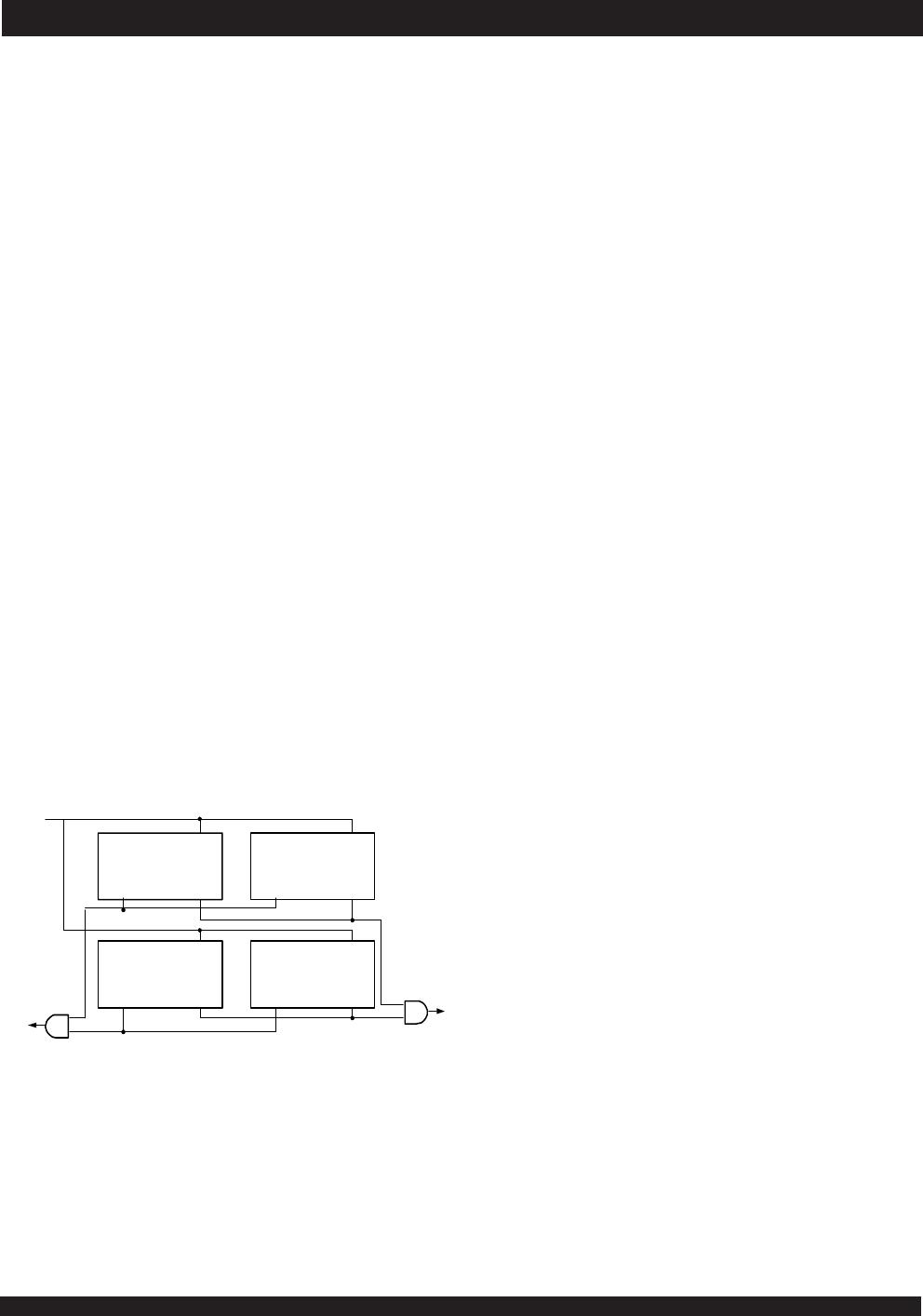
reason for this is easily understood by looking at the simple logic diagram
of the semaphore flag in Figure 4. Two semaphore request latches feed
into a semaphore flag. Whichever latch is first to present a zero to the
semaphore flag will force its side of the semaphore flag LOW and the other
side HIGH. This condition will continue until a one is written to the same
semaphore request latch. Should the other side’s semaphore request latch
have been written to a zero in the meantime, the semaphore flag will flip
over to the other side as soon as a one is written into the first side’s request
latch. The second side’s flag will now stay LOW until its semaphore request
latch is written to a one. From this it is easy to understand that, if a semaphore
is requested and the processor which requested it no longer needs the
resource, the entire system can hang up until a one is written into that
The critical case of semaphore timing is when both sides request a
single token by attempting to write a zero into it at the same time. The
semaphore logic is specially designed to resolve this problem. If simulta-
neous requests are made, the logic guarantees that only one side receives
the token. If one side is earlier than the other in making the request, the first
side to make the request will receive the token. If both requests arrive at
the same time, the assignment will be arbitrarily made to one port or the
other.
One caution that should be noted when using semaphores is that
semaphores alone do not guarantee that access to a resource is secure.
As with any powerful programming technique, if semaphores are misused
or misinterpreted, a software error can easily happen.
Initialization of the semaphores is not automatic and must be handled
via the initialization program at power-up. Since any semaphore request
flag which contains a zero must be reset to a one, all semaphores on both
sides should have a one written into them at initialization from both sides
to assure that they will be free when needed.
How the Semaphore Flags Work
The semaphore logic is a set of eight latches which are independent
of the Dual-Port RAM. These latches can be used to pass a flag, or token,
from one port to the other to indicate that a shared resource
is in use. The semaphores provide a hardware assist for a use assignment
method called “Token Passing Allocation.” In this method, the state of a
semaphore latch is used as a token indicating that a shared resource is
in use. If the left processor wants to use this resource, it requests the token
by setting the latch. This processor then verifies its success in setting the
latch by reading it. If it was successful, it proceeds to assume control over
the shared resource. If it was not successful in setting the latch, it determines
that the right side processorhas set the latch first, has the token and is using
the shared resource. The left processor can then either repeatedly request
that semaphore’s status or remove its request for that semaphore to
perform another task and occasionally attempt again to gain control of the
token via the set and test sequence. Once the right side has relinquished
the token, the left side should succeed in gaining control.
Figure 4. IDT70V659/58/57 Semaphore Logic
D
4869 drw 1
9
0
D
Q
WRITE
D
0
D
Q
WRITE
SEMAPHORE
REQUEST FLIP FLOP
SEMAPHORE
REQUEST FLIP FLOP
LPORT
RPORT
SEMAPHORE
READ
SEMAPHORE
READ
request latch will contain a zero, yet the semaphore flag will appear as one,
a fact which the processor will verify by the subsequent read (see Table
V). As an example, assume a processor writes a zero to the left port at a
free semaphore location. On used instead, system contention problems
could have occurred during the gap between the read and write cycles.
It is important to note that a failed semaphore request must be followed
by either repeated reads or by writing a one into the same location. The
semaphore request latch.

70V658S15BC8

Mfr. #:
Manufacturer:
IDT
Description:
SRAM 64Kx36 STD-PWR, 3.3V DUAL-PORT RAM
Lifecycle:
New from this manufacturer.
Delivery:
DHL FedEx Ups TNT EMS
Payment:
T/T Paypal Visa MoneyGram Western Union