2
LTC1404
1404fa
The ● denotes specifications which apply over the full operating temperature range, unless otherwise
noted specifications are at T
A
= 25°C. V
CC
= 5V, f
SAMPLE
= 600kHz, t
r
= t
f
= 5ns, unless otherwise specified.
ABSOLUTE MAXIMUM RATINGS
W
WW
U
(Notes 1, 2)
Supply Voltage (V
CC
) ................................................. 7V
Negative Supply Voltage (V
SS
) ................... – 6V to GND
Total Supply Voltage (V
CC
to V
SS
)
Bipolar Operation Only ........................................ 12V
Analog Input Voltage (Note 3)
Unipolar Operation .................. –0.3V to (V
CC
+ 0.3V)
Bipolar Operation........... (V
SS
– 0.3V) to (V
CC
+ 0.3V)
Digital Input Voltage (Note 4)
Unipolar Operation ................................– 0.3V to 12V
Bipolar Operation.........................(V
SS
– 0.3V) to 12V
Digital Output Voltage
Unipolar Operation .................. –0.3V to (V
CC
+ 0.3V)
Bipolar Operation........... (V
SS
– 0.3V) to (V
CC
+ 0.3V)
Power Dissipation.............................................. 300mW
Operating Ambient Temperature Range
LTC1404C ............................................... 0°C to 70°C
LTC1404I............................................ –40°C to 85°C
Junction Temperature.......................................... 125°C
Storage Temperature Range ................. –65°C to 150°C
Lead Temperature (Soldering, 10 sec).................. 300°C
PACKAGE/ORDER INFORMATION
W
U
U
SYMBOL PARAMETER CONDITIONS MIN TYP MAX UNITS
V
CC
Positive Supply Voltage Unipolar 4.75 5.25 V
Bipolar 4.75 5.25 V
V
SS
Negative Supply Voltage Bipolar Only –2.45 –5.25 V
I
CC
Positive Supply Current f
SAMPLE
= 600ksps ● 15 30 mA
Nap Mode
● 1.3 3.0 mA
Sleep Mode ● 8.0 20.0 µA
I
SS
Negative Supply Current f
SAMPLE
= 600ksps, V
SS
= – 5V ● 0.2 0.6 mA
Nap Mode
● 0.2 0.5 mA
Sleep Mode ● 410 µA
P
D
Power Dissipation f
SAMPLE
= 600ksps ● 75 160 mW
Nap Mode
● 7.5 20 mW
Sleep Mode ● 60 150 µW
SYMBOL PARAMETER CONDITIONS MIN TYP MAX UNITS
V
IN
Analog Input Range 4.75V ≤ V
CC
≤ 5.25V (Unipolar) 0 to 4.096 V
4.75V ≤ V
CC
≤ 5.25V, –5.25V ≤ V
SS
≤ – 2.45V (Bipolar) 0 to ±2.048 V
I
IN
Analog Input Leakage Current During Conversions (Hold Mode) ● ±1 µA
C
IN
Analog Input Capacitance Between Conversions (Sample Mode) 45 pF
During Conversions (Hold Mode) 5 pF
PUT
U
IA
A
U
LOG
POWER REQUIRE E TS
W
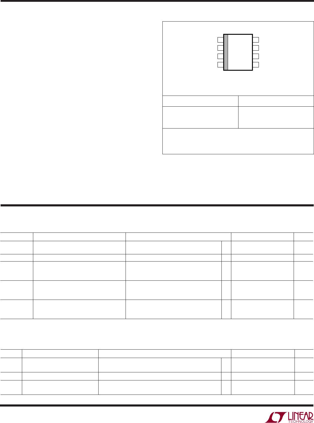
U
TOP VIEW
V
CC
A
IN
V
REF
GND
V
SS
CONV
CLK
D
OUT
S8 PACKAGE
8-LEAD PLASTIC SO
1
2
3
4
8
7
6
5
T
JMAX
= 125°C, θ
JA
= 130°C/W
ORDER PART NUMBER
S8 PART MARKING
Consult LTC Marketing for parts specified with wider operating temperature ranges.
LTC1404CS8
LTC1404IS8
1404
1404I
Order Options Tape and Reel: Add #TR
Lead Free: Add #PBF Lead Free Tape and Reel: Add #TRPBF
Lead Free Part Marking: http://www.linear.com/leadfree/
The
● denotes specifications which apply over the full operating temperature range,
unless otherwise noted specifications are at T
A
= 25°C. V
CC
= 5V, f
SAMPLE
= 600kHz, t
r
= t
f
= 5ns, unless otherwise specified.