16
LTC1404
1404fa
APPLICATIONS INFORMATION
WUU
U
inputs must be within 500mV of the supply rails). In Sleep
mode, power consumption is reduced to 60µW by cutting
off power to all internal circuitry including the reference.
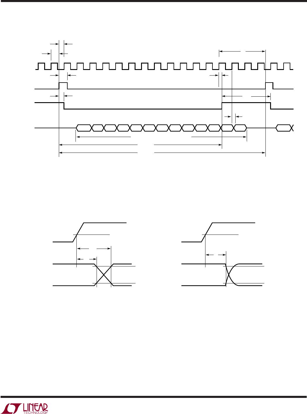
Figure 12 illustrates power-down modes for the LTC1404.
The chip enters Nap mode by keeping the CLK signal low
and pulsing the CONV signal twice. For Sleep mode
operation, the CONV signal should be pulsed four times
while CLK is kept low. Nap and Sleep modes are activated
on the falling edge of the CONV pulse.
The LTC1404 returns to active mode easily. The rising
edge of CLK wakes up the LTC1404. From Nap mode,
wake-up occurs within 350ns. During the transition from
Sleep mode to active mode, the V
REF
voltage ramp-up time
is a function of its loading conditions. With a 10µF bypass
capacitor, the wake-up time from Sleep mode is typically
2.5ms. A REFRDY signal is activated once the reference
has settled and is ready for an A/D conversion. This
REFRDY bit is sent to the D
OUT
pin as the first bit followed
by the 12-bit data word (refer to Figure 13). To save power
during wake-up from Sleep mode, the chip is designed to
enter Nap mode automatically until the reference is ready.
Once REFRDY goes high, the comparator powers up
immediately and is ready for a conversion. During the Nap
interval, any attempt to perform an analog-to-digital con-
version will result in an all-zero output code, including the
REFRDY bit. If no conversion is attempted, the D
OUT
pin
remains in a high impedance state. If the ADC wakes from
Sleep mode, this can be determined by monitoring the
state of the REFRDY bit at the D
OUT
pin.
DIGITAL INTERFACE
The digital interface requires only three digital lines. CLK
and CONV are both inputs, and the D
OUT
output provides
the conversion result in serial form.
Figure 13 shows the digital timing diagram of the LTC1404
during the A/D conversion. The CONV rising edge starts
the conversion. Once initiated, it can not be restarted until
the conversion is completed. If the time from CONV signal
to CLK rising edge is less than t
2,
the digital output will be
delayed by one clock cycle.
The digital output data is updated on the rising edge of the
CLK line. The digital output data consists of a REFRDY bit
followed by a valid 12-bit data word. D
OUT
data should be
captured by the receiving system on the rising CLK edge.
Data remains valid for a minimum time of t
10
after the
rising CLK edge to allow capture to occur.
Figure 12. Nap Mode and Sleep Mode Waveforms
CLK
CONV
NAP
SLEEP
V
REF
t
1
t
1
t
11
REFRDY
Hi-Z Hi-Z Hi-Z Hi-Z
ALL ZERO
REFRDY BIT+12-BIT
DATA WORD
REFRDY = 0
D
OUT
NOTE: NAP AND SLEEP ARE INTERNAL SIGNALS.
REFRDY APPEARS AS THE FIRST BIT IN THE D
OUT
WORD
10
10
11
1
1404 F12
REFRDY BIT
+12-BIT
DATA WORD
REFRDY = 1
t
11