10
LTC1404
1404fa
APPLICATIONS INFORMATION
WUU
U
Dynamic Performance
The LTC1404 has excellent high speed sampling capabil-
ity. FFT (Fast Fourier Transform) test techniques are used
to test the ADC’s frequency response, distortion and noise
at the rated throughput. By applying a low distortion sine
wave and analyzing the digital output using an FFT algo-
rithm, the ADC’s spectral content can be examined for
frequencies outside the fundamental. Figure 2a shows a
typical LTC1404 FFT plot.
Conversion Details
The LTC1404 uses a successive approximation algorithm
and an internal sample-and-hold circuit to convert an
analog signal to a 12-bit serial output based on a precision
internal reference. The control logic provides easy inter-
face to microprocessors and DSPs through 3-wire con-
nections.
A rising edge on the CONV input starts a conversion. At the
start of a conversion the successive approximation regis-
ter (SAR) is reset. Once a conversion cycle has begun, it
cannot be restarted.
During conversion, the internal 12-bit capacitive DAC
output is sequenced by the SAR from the most significant
bit (MSB) to the least significant bit (LSB). Referring to
Figure 1, the A
IN
input connects to the sample-and-hold
capacitor during the acquired phase and the comparator
offset is nulled by the feedback switch. In this acquire
phase, it typically takes 160ns for the sample-and-hold
capacitor to acquire the analog signal. During the convert
phase, the comparator feedback switch opens, putting the
comparator into the compare mode. The input switches
connect C
SAMPLE
to ground, injecting the analog input
charge onto the summing junction. This input charge is
successively compared with the binary-weighted charges
supplied by the capacitive DAC. Bit decisions are made by
the high speed comparator. At the end of a conversion, the
DAC output balances the A
IN
input charge. The SAR
contents (a 12-bit data word) which represent the input
voltage, are presented through the serial pin D
OUT
.
1404 F01
SAMPLE
D
OUT
C
DAC
V
DAC
DAC
A
IN
C
SAMPLE
+
COMP
S
A
R
SAMPLE
S1
HOLD
Figure 1. A
IN
Input
FREQUENCY (kHz)
0 60 90 120 150 180 210 240 270 300
AMPLITUDE (dB)
1404 F02a
0
–10
–20
–30
–40
–50
–60
–70
–80
–90
100
110
120
30
f
SAMPLE
= 600kHz
f
IN
= 99.169kHz
SINAD = 72dB
THD = –88dB
Figure 2a. LTC1404 Nonaveraged, 4096 Point FFT
Plot with 100kHz Input Frequency in Bipolar Mode
Figure 2b. LTC1404 Nonaveraged, 4096 Point FFT
Plot with 300kHz Input Frequency in Bipolar Mode
FREQUENCY (kHz)
0 60 90 120 150 180 210 240 270 300
AMPLITUDE (dB)
1404 F02b
0
–10
–20
–30
–40
–50
–60
–70
–80
–90
100
110
120
30
f
SAMPLE
= 600kHz
f
IN
= 298.681kHz
SINAD = 71dB
THD = –84dB
11
LTC1404
1404fa
APPLICATIONS INFORMATION
WUU
U
Signal-to-Noise Ratio
The signal-to-noise plus distortion ratio [S/(N + D)] is the
ratio between the RMS amplitude of the fundamental input
frequency to the RMS amplitude of all other frequency
components at the A/D output. The output is band limited
to frequencies from DC to half the sampling frequency.
Figure 2a shows a typical spectral content with a 600kHz
sampling rate and a 100kHz input. The dynamic perfor-
mance is excellent for input frequencies up to the Nyquist
limit of 300kHz as shown in Figure 2b.
Effective Number of Bits
The effective number of bits (ENOBs) is a measurement of
the effective resolution of an ADC and is directly related to
the S/(N + D) by the equation:
N
SN D
=
+
()
/–.
.
176
602
where N is the effective number of bits of resolution and
S/(N + D) is expressed in dB. At the maximum sampling
rate of 600kHz, the LTC1404 maintains very good ENOBs
up to the Nyquist input frequency of 300kHz (refer to
Figure 3).
Total Harmonic Distortion
Total harmonic distortion (THD) is the ratio of the RMS
sum of all harmonics of the input signal to the fundamental
itself. The out-of-band harmonics alias into the frequency
band between DC and half of the sampling frequency. THD
is expressed as:
THD
VVV Vn
V
=
+++
20
234
1
222 2
log
where V1 is the RMS amplitude of the fundamental fre-
quency and V2 through Vn are the amplitudes of the
second through nth harmonics. THD vs input frequency is
shown in Figure 4. The LTC1404 has good distortion
performance up to the Nyquist frequency and beyond.
INPUT FREQUENCY (Hz)
10k
AMPLITUDE (dB BELOW THE FUNDAMENTAL)
0
–10
–20
–30
–40
–50
–60
–70
–80
–90
100
100k 1M
1404 F04
f
SAMPLE
= 600kHz
3RD HARMONIC
THD
2ND HARMONIC
Figure 4. Distortion vs Input Frequency in
Bipolar Mode
Intermodulation Distortion
If the ADC input signal consists of more than one spectral
component, the ADC transfer function nonlinearity can
produce intermodulation distortion (IMD) in addition to
THD. IMD is the change in one sinusoidal input caused by
the presence of another sinusoidal input at a different
frequency.
INPUT FREQUENCY (Hz)
10k
EFFECTIVE NUMBER OF BITS
SIGNAL/(NOISE + DISTORTION) (dB)
12
11
10
9
8
7
6
5
4
3
2
1
0
74
68
62
56
50
100k 1M
1404 F03
NYQUIST
FREQUENCY
f
SAMPLE
= 600kHz
Figure 3. Effective Bits and Signal-to-Noise +
Distortion vs Input Frequency in Bipolar Mode
12
LTC1404
1404fa
APPLICATIONS INFORMATION
WUU
U
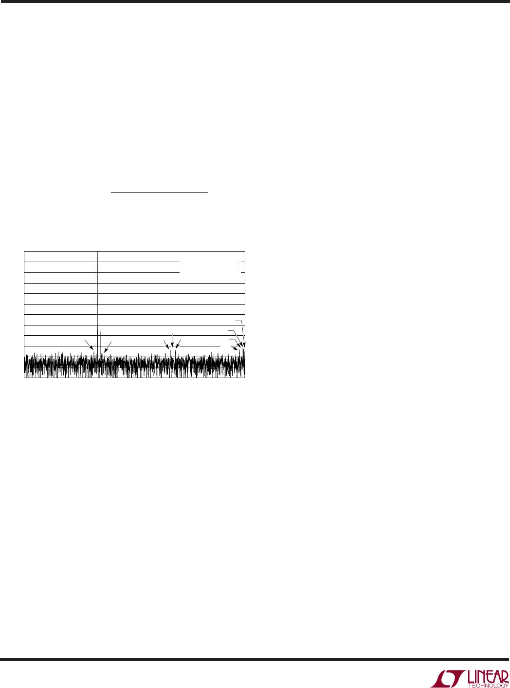
If two pure sine waves of frequencies fa and fb are applied
to the ADC input, nonlinearities in the ADC transfer func-
tion can create distortion products at sum and difference
frequencies of mfa ± nfb, where m and n = 0, 1, 2, 3, etc.
For example, the 2nd order IMD terms include (fa + fb) and
(fa – fb) while the 3rd order IMD terms includes (2fa + fb),
(2fa – fb), (fa + 2fb) and (fa – 2fb). If the two input sine
waves are equal in magnitude, the value (in decibels) of the
2nd order IMD products can be expressed by the following
formula.
IMD fa fb
fa fb
±
()
=
±
20log
Amplitude at ( )
Amplitude at fa
Figure 5 shows the IMD performance at a 100kHz input.
Figure 5. Intermodulation Distortion Plot in Bipolar Mode
FREQUENCY (kHz)
0 40 80 100 140 18020 60 120 160 220200 240 260 280 300
AMPLITUDE (dB)
1404 F05
0
–10
–20
–30
–40
–50
–60
–70
–80
–90
100
110
120
f
SAMPLE
= 600kHz
fa = 99.16992188kHz
fb = 102.6855469kHz
fa fb
3fa
2fb – fa
2fa – fb
2fa + fb
2fa
3fb
fa + fb
2fb
2fb + fa
Peak Harmonic or Spurious Noise
The peak harmonic or spurious noise is the largest spec-
tral component excluding the input signal and DC. This
value is expressed in decibels relative to the RMS value of
a full-scale input signal.
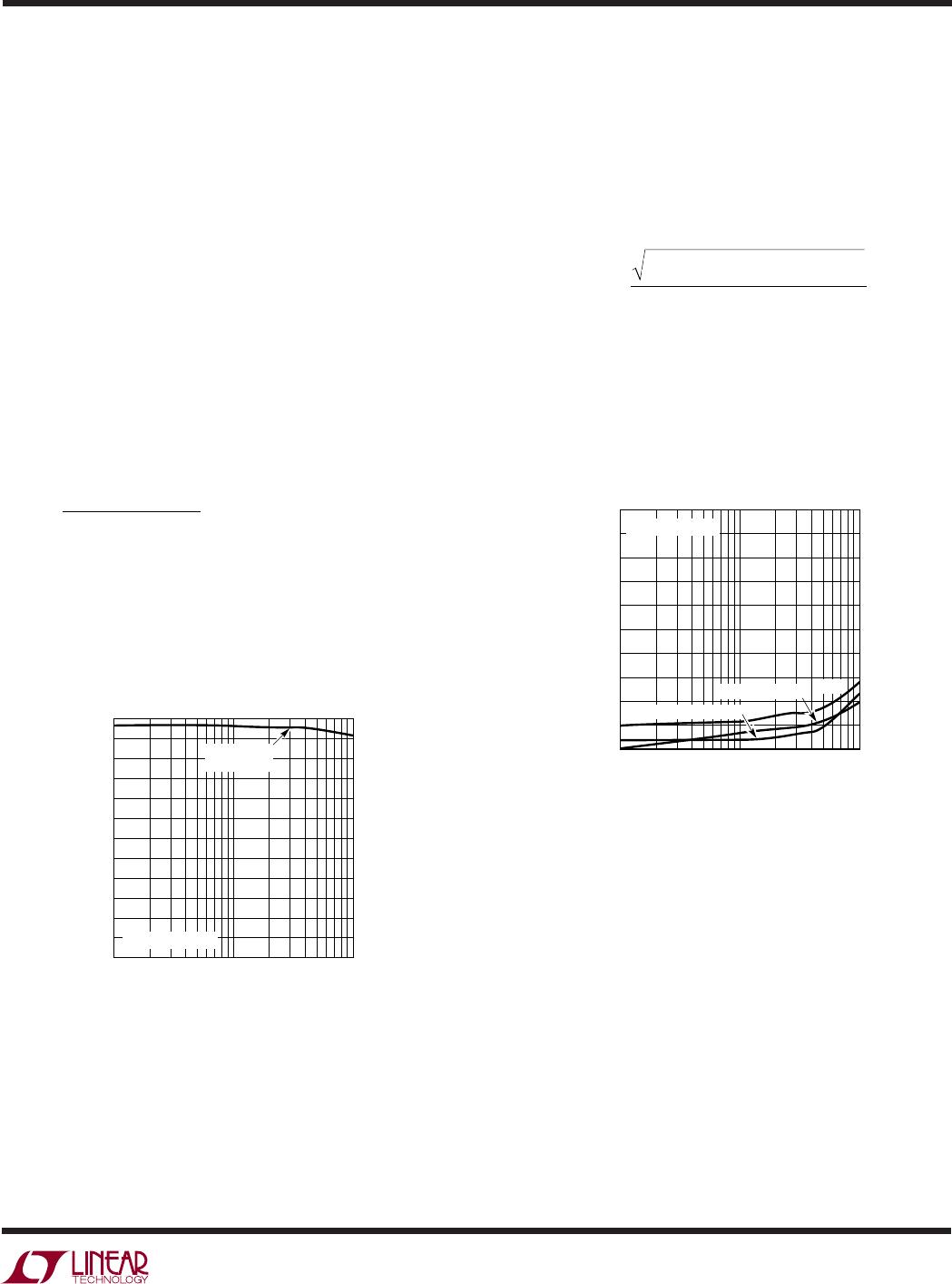
Full Power and Full Linear Bandwidth
The full power bandwidth is the input frequency at which
the amplitude of the reconstructed fundamental is re-
duced by 3dB for a full-scale input signal.
The full linear bandwidth is the input frequency at which
the S/(N + D) has dropped to 68dB (11 effective bits). The
LTC1404 has been designed to optimize input bandwidth,
allowing the ADC to undersample input signals with fre-
quencies above the converter’s Nyquist Frequency. The
noise floor stays very low at high frequencies; S/(N + D)
becomes dominated by distortion at frequencies far be-
yond Nyquist.
Driving the Analog Input
The analog input of the LTC1404 is easy to drive. It draws
only one small current spike while charging the sample-
and-hold capacitor at the end of a conversion. During
conversion, the analog input draws only a small leakage
current. The only requirement is that the amplifier driving
the analog input must settle after the small current spike
before the next conversion starts. Any op amp that settles
in 160ns to small load current transient will allow maxi-
mum speed operation. If a slower op amp is used, more
settling time can be provided by increasing the time
between conversions. Suitable devices capable of driving
the ADC’s A
IN
input include the LT
®
1360 and the LT1363
op amps.
The LTC1404 comes with a built-in unipolar/bipolar detec-
tion circuit. If the V
SS
potential is forced below GND, the
internal circuitry will automatically switch to bipolar mode.
The following
list is a summary of the op amps that are
suitable for driving the LTC1404, more detailed informa-
tion is available in the Linear Technology databooks or the
Linear Technology Web site.
LT 1215/LT1216: Dual and quad 23MHz, 50V/µs single
supply op amps. Single 5V to ±15V supplies, 6.6mA
specifications, 90ns settling to 0.5LSB.
LT1223: 100MHz video current feedback amplifier. ±5V
to ±15V supplies, 6mA supply current. Low distortion up
to and above 600kHz. Low noise. Good for AC applica-
tions.
LT1227: 140MHz video current feedback amplifier. ±5V
to ±15V supplies, 10mA supply current. Lowest distor-
tion at frequencies above 600kHz. Low noise. Best for AC
applications.

LTC1404CS8#PBF

Mfr. #:
Manufacturer:
Analog Devices Inc.
Description:
Analog to Digital Converters - ADC Complete SO-8, 12-B, 600ksps ADC w/ SD
Lifecycle:
New from this manufacturer.
Delivery:
DHL FedEx Ups TNT EMS
Payment:
T/T Paypal Visa MoneyGram Western Union