OP1177/OP2177/OP4177
Rev. G | Page 16 of 24
OP1177
6
7
2
3
4
V+
V–
R2
100k
V
OUT
10k
R1
1k
+
2
00m
V
02627-054
Figure 54. Test Circuit for Overload Recovery Time
Figure 18 shows the positive overload recovery time of the
OP1177. The output recovers in less than 4 µs after being
overdriven by more than 100%.
The negative overload recovery of the OP1177 is 1.4 µs, as seen
in Figure 19.
THD + NOISE
The OPx177 has very low total harmonic distortion. This indicates
excellent gain linearity and makes the OPx177 a great choice for
high closed-loop gain precision circuits.
Figure 55 shows that the OPx177 has approximately 0.00025%
distortion in unity gain, the worst-case configuration for distortion.
FREQUENCY (Hz)
THD + N (%)
100 1k
0.001
0.01
20 6k
0.0001
0.1
02627-055
V
SY
= ±15V
R
L
= 10k
BW = 22kHz
Figure 55. THD + N vs. Frequency
CAPACITIVE LOAD DRIVE
OPx177 is inherently stable at all gains and capable of driving
large capacitive loads without oscillation. With no external
compensation, the OPx177 safely drives capacitive loads up to
1000 pF in any configuration. As with virtually any amplifier,
driving larger capacitive loads in unity gain requires additional
circuitry to assure stability.
In this case, a snubber network is used to prevent oscillation
and reduce the amount of overshoot. A significant advantage of
this method is that it does not reduce the output swing because
the Resistor R
S
is not inside the feedback loop.
Figure 56 is a scope shot of the output of the OPx177 in response
to a 400 mV pulse. The load capacitance is 2 nF. The circuit is
configured in positive unity gain, the worst-case condition for
stability.
As shown in Figure 58, placing an R-C network parallel to the
load capacitance (C
L
) allows the amplifier to drive higher values
of C
L
without causing oscillation or excessive overshoot.
There is no ringing, and overshoot is reduced from 27% to 5%
using the snubber network.
Optimum values for R
S
and C
S
are tabulated in Table 5 for several
capacitive loads, up to 200 nF. Values for other capacitive loads can
be determined experimentally.
Table 5. Optimum Values for Capacitive Loads
C
L
R
S
C
S
10 nF 20 Ω 0.33 µF
50 nF 30 Ω 6.8 nF
200 nF 200 Ω 0.47 µF
0
GND
VOLTAGE (200mV/DIV)
TIME (10µs/DIV)
V
SY
= ±5V
R
L
= 10k
C
L
= 2nF
0
2627-056
Figure 56. Capacitive Load Drive Without Snubber
GND
VOL
T
AGE (200mV/DIV)
TIME (10µs/DIV)
V
SY
= ±5V
R
L
= 10k
R
S
= 200
C
L
= 2nF
C
S
= 0.47µF
0
2627-057
Figure 57. Capacitive Load Drive with Snubber
OP1177/OP2177/OP4177
Rev. G | Page 17 of 24
OP1177
6
7
2
3
4
V+
V–
V
OUT
R
S
+
400mV
C
S
C
L
0
2627-058
Figure 58. Snubber Network Configuration
Caution: The snubber technique cannot recover the loss of
bandwidth induced by large capacitive loads.
STRAY INPUT CAPACITANCE COMPENSATION
The effective input capacitance in an operational amplifier
circuit (C
t
) consists of three components. These are the internal
differential capacitance between the input terminals, the internal
common-mode capacitance of each input to ground, and the
external capacitance including parasitic capacitance. In the
circuit in Figure 59, the closed-loop gain increases as the signal
frequency increases.
The transfer function of the circuit is
()
R1sC
R1
R2
t
++ 1 1
indicating a zero at
()
tt
CR2R1R2R1C
R1R2
s
/ 2
1
π
=
+
=
Depending on the value of R1 and R2, the cutoff frequency of
the closed-loop gain can be well below the crossover frequency.
In this case, the phase margin (Φ
M
) can be severely degraded,
resulting in excessive ringing or even oscillation.
A simple way to overcome this problem is to insert a capacitor
in the feedback path, as shown in Figure 60.
The resulting pole can be positioned to adjust the phase margin.
Setting C
f
= (R1/R2) C
t
achieves a phase margin of 90°.
R2R1
V1
+
OP1177
2
3
V
OUT
C
t
02627-059
6
7
4
V+
V–
Figure 59. Stray Input Capacitance
R2R1
V1
+
OP1177
2
3
V
OUT
C
t
C
f
02627-060
6
7
4
V+
V–
Figure 60. Compensation Using Feedback Capacitor
REDUCING ELECTROMAGNETIC INTERFERENCE
A number of methods can be utilized to reduce the effects of
EMI on amplifier circuits.
In one method, stray signals on either input are coupled to the
opposite input of the amplifier. The result is that the signal is
rejected according to the CMRR of the amplifier.
This is usually achieved by inserting a capacitor between the inputs
of the amplifier, as shown in Figure 61. However, this method can
also cause instability, depending on the value of capacitance.
R2R1
V1
+
OP1177
2
3
V
OUT
C
02627-061
6
7
4
V+
V–
Figure 61. EMI Reduction
Placing a resistor in series with the capacitor (see Figure 62)
increases the dc loop gain and reduces the output error. Positioning
the breakpoint (introduced by R-C) below the secondary pole of
the operational amplifier improves the phase margin and,
therefore, stability.
R can be chosen independently of C for a specific phase margin
according to the formula
()
+=
R1
R2
jfa
R2
R
2
1
where:
a is the open-loop gain of the amplifier.
f
2
is the frequency at which the phase of a = Φ
M
− 180°.
OP1177
2
3
R
C
R1
R2
V
OUT
V1
+
02627-062
6
7
4
V+
V–
Figure 62. Compensation Using Input R-C Network
OP1177/OP2177/OP4177
Rev. G | Page 18 of 24
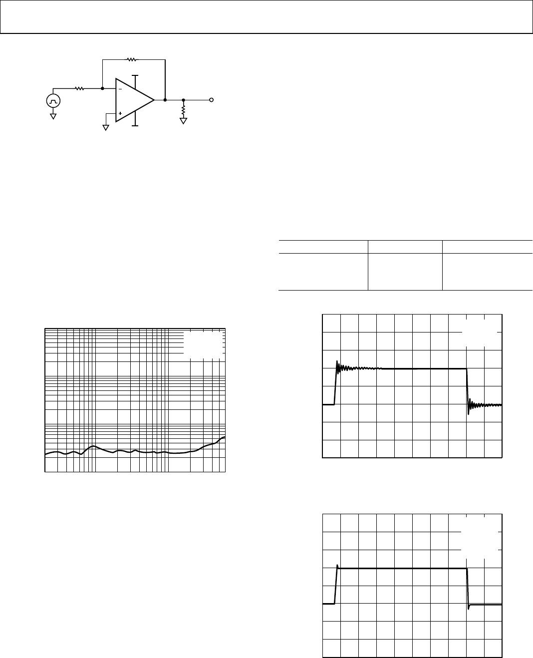
PROPER BOARD LAYOUT
The OPx177 is a high precision device. To ensure optimum
performance at the PCB level, care must be taken in the design
of the board layout.
To avoid leakage currents, the surface of the board should be
kept clean and free of moisture. Coating the surface creates a
barrier to moisture accumulation and helps reduce parasitic
resistance on the board.
Keeping supply traces short and properly bypassing the power
supplies minimizes power supply disturbances due to output
current variation, such as when driving an ac signal into a heavy
load. Bypass capacitors should be connected as closely as possible
to the device supply pins. Stray capacitances are a concern at the
outputs and the inputs of the amplifier. It is recommended that
signal traces be kept at least 5 mm from supply lines to
minimize coupling.
A variation in temperature across the PCB can cause a mismatch in
the Seebeck voltages at solder joints and other points where dissi-
milar metals are in contact, resulting in thermal voltage errors. To
minimize these thermocouple effects, orient resistors so heat
sources warm both ends equally. Input signal paths should contain
matching numbers and types of components, where possible to
match the number and type of thermocouple junctions. For
example, dummy components such as zero value resistors can
be used to match real resistors in the opposite input path.
Matching components should be located in close proximity and
should be oriented in the same manner. Ensure leads are of equal
length so that thermal conduction is in equilibrium. Keep heat
sources on the PCB as far away from amplifier input circuitry as
is practical.
The use of a ground plane is highly recommended. A ground
plane reduces EMI noise and also helps to maintain a constant
temperature across the circuit board.
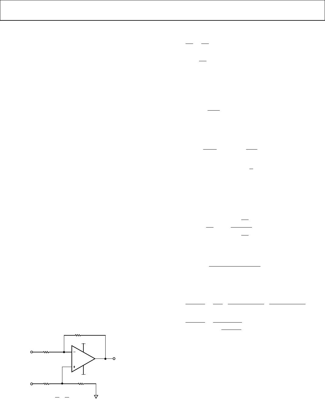
DIFFERENCE AMPLIFIERS
Difference amplifiers are used in high accuracy circuits to improve
the common-mode rejection ratio (CMRR).
R1
V
1
V
2
R3 = R1
R4 = R1
OP1177
2
3
=
R4
R3
R2
R1
R2
100k
V
OUT
02627-063
6
7
4
V+
V–
Figure 63. Difference Amplifier
In the single instrumentation amplifier (see Figure 63), where
R1
R2
R3
R4
=
()
12
O
VV
R1
R2
V =
a mismatch between the ratio R2/R1 and R4/R3 causes the
common-mode rejection ratio to be reduced.
To better understand this effect, consider that, by definition,
CM
DM
A
A
CMRR =
where ADM is the differential gain and ACM is the common-
mode gain.
CM
O
CM
DIFF
O
DM
V
V
A
V
V
A and ==
()
21
CM
21
DIFF
VVVVVV +==
2
1
and
For this circuit to act as a difference amplifier, its output must
be proportional to the differential input signal.
From Figure 63,
21
O
V
R4
R3
R1
R2
V
R1
R2
V
1
1
+
+
+
=
Arranging terms and combining the previous equations yields
R2R3R4R1
R4R2R3R2R4R1
CMRR
22
2
+
+
=
(1)
The sensitivity of CMRR with respect to the R1 is obtained by
taking the derivative of CMRR, in Equation 1, with respect to R1.
+
+
δ
δ
=
δ
δ
R2R3R1R4
R2R3R2R4
R2R3R1R4
R1R4
R1R1
CMRR
22
2
22
()
R1R4
R2R3
R1
CMRR
2
2
1
=
δ
δ
Assuming that
R1R2R3R4R
and
R(1 − δ) < R1, R2, R3, R4 < R(1 + δ)
the worst-case CMRR error arises when
R1 = R4 = R(1 + δ) and R2 = R3 = R(1 − δ)

OP1177ARZ-REEL7

Mfr. #:
Manufacturer:
Analog Devices Inc.
Description:
Precision Amplifiers Low Noise Low Input Bias Current SGL IC
Lifecycle:
New from this manufacturer.
Delivery:
DHL FedEx Ups TNT EMS
Payment:
T/T Paypal Visa MoneyGram Western Union