OP1177/OP2177/OP4177
Rev. G | Page 19 of 24
Plugging these values into Equation 1 yields
δ
2
1
MIN
CMRR
where δ is the tolerance of the resistors.
Lower tolerance value resistors result in higher common-mode
rejection (up to the CMRR of the operational amplifier).
Using 5% tolerance resistors, the highest CMRR that can be
guaranteed is 20 dB. Alternatively, using 0.1% tolerance resistors
results in a common-mode rejection ratio of at least 54 dB
(assuming that the operational amplifier CMRR × 54 dB).
With the CMRR of OPx177 at 120 dB minimum, the resistor
match is the limiting factor in most circuits. A trimming resistor
can be used to further improve resistor matching and CMRR of
the difference amplifier circuit.
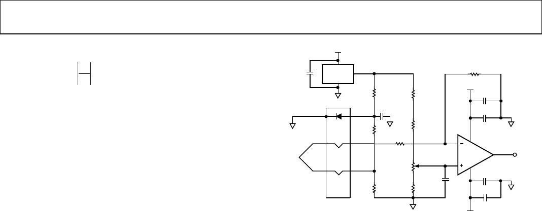
A HIGH ACCURACY THERMOCOUPLE AMPLIFIER
A thermocouple consists of two dissimilar metal wires placed in
contact. The dissimilar metals produce a voltage
V
TC
= α(T
J
T
R
)
where:
T
J
is the temperature at the measurement of the hot junction.
T
R
is the temperature at the cold junction.
α is the Seebeck coefficient specific to the dissimilar metals used
in the thermocouple.
V
TC
is the thermocouple voltage and becomes larger with
increasing temperature.
Maximum measurement accuracy requires cold junction compen-
sation of the thermocouple. To perform the cold junction compen-
sation, apply a copper wire short across the terminating junctions
(inside the isothermal block) simulating a 0°C point. Adjust the
output voltage to zero using the R5 trimming resistor, and remove
the copper wire.
The OPx177 is an ideal amplifier for thermocouple circuits
because it has a very low offset voltage, excellent PSRR and
CMRR, and low noise at low frequencies.
It can be used to create a thermocouple circuit with great
linearity. Resistor R1, Resistor R2, and Diode D1, shown in
Figure 64, are mounted in an isothermal block.
V+
7
4
Cu
Cu
TR
TR
D1
D1
ADR293
V
CC
C1
2.2µF
R3
47k
10µF
R2
4.02k
R8
1k
R7
80.6k
R6
50
R9
200k
0.1µF
10µF
0.1µF
10µF
V–
10µF
R4
50
R5
100
R1
50
ISOTHERMAL
BLOCK
V
TC
T
J
(–)
(+)
6
2
3
OP1177
V
OUT
02627-064
Figure 64. Type K Thermocouple Amplifier Circuit
LOW POWER LINEARIZED RTD
A common application for a single element varying bridge is an
RTD thermometer amplifier, as shown in Figure 65. The excita-
tion is delivered to the bridge by a 2.5 V reference applied at the
top of the bridge.
RTDs may have thermal resistance as high as 0.5°C to 0.8°C
per mW. To minimize errors due to resistor drift, the current
through each leg of the bridge must be kept low. In this circuit,
the amplifier supply current flows through the bridge. However,
at the OPx177 maximum supply current of 600 µA, the RTD
dissipates less than 0.1 mW of power, even at the highest resis-
tance. Errors due to power dissipation in the bridge are kept
under 0.1°C.
Calibration of the bridge is made at the minimum value of
temperature to be measured by adjusting R
P
until the output is zero.
To calibrate the output span, set the full-scale and linearity
potentiometers to midpoint and apply a 500°C temperature to
the sensor or substitute the equivalent 500°C RTD resistance.
Adjust the full-scale potentiometer for a 5 V output. Finally,
apply 250°C or the equivalent RTD resistance and adjust the
linearity potentiometer for 2.5 V output. The circuit achieves
better than ±0.5°C accuracy after adjustment.
OP1177/OP2177/OP4177
Rev. G | Page 20 of 24
0
2627-065
200
500
4.37k
100
100 20
4.12k
4.12k
5k
49.9k
ADR421
+15
V
0.1µ
F
V+
100
RTD
1/2
OP2177
7
6
5
1/2
OP2177
1
8
2
3
4
V–
V
OU
T
V
OUT
where δ = ∆R/R is the fractional deviation of the RTD resistance
with respect to the bridge resistance due to the change in temper-
ature at the RTD.
For δ << 1, the preceding expression becomes
δ
+
+
=
++
δ
REF
REF
O
V
R2
R1
R2
R1
R
R2
R2
R1
R
R1
V
R
R2
V
1
1
With V
REF
constant, the output voltage is linearly proportional
to δ with a gain factor of
+
+
R2
R1
R2
R1
R
R2
V
REF
1
02627-066
R
R
R
R(1+δ)
ADR421
15V
0.1µ
F
OP1177
6
7
4
2
3
V+
V–
R
F
R
F
V
OUT
Figure 65. Low Power Linearized RTD Circuit
SINGLE OPERATIONAL AMPLIFIER BRIDGE
The low input offset voltage drift of the OP1177 makes it very
effective for bridge amplifier circuits used in RTD signal condi-
tioning. It is often more economical to use a single bridge
operational amplifier as opposed to an instrumentation amplifier.
In the circuit shown in Figure 66, the output voltage at the
operational amplifier is
Figure 66. Single Bridge Amplifier
()
δ+
++
δ
=
1 1
R2
R1
R
R1
V
R
R2
V
REF
O
OP1177/OP2177/OP4177
Rev. G | Page 21 of 24
REALIZATION OF ACTIVE FILTERS
BAND-PASS KRC OR SALLEN-KEY FILTER
The low offset voltage and the high CMRR of the OPx177 make
it an excellent choice for precision filters, such as the band-pass
KRC filter shown in Figure 67. This filter type offers the capability
to tune the gain and the cutoff frequency independently.
Because the common-mode voltage into the amplifier varies with
the input signal in the KRC filter circuit, a high CMRR is required
to minimize distortion. Also, the low offset voltage of the OPx177
allows a wider dynamic range when the circuit gain is chosen to
be high.
The circuit of Figure 67 consists of two stages. The first stage is
a simple high-pass filter where the corner frequency (f
C
) is
C1C2R1R2π2
1
(2)
and
R2
R1
KQ =
(3)
where K is the dc gain.
Choosing equal capacitor values minimizes the sensitivity and
simplifies Equation 2 to
R1R2C
π
2
1
The value of Q determines the peaking of the gain vs. frequency
(ringing in transient response). Commonly chosen values for Q
are generally near unity.
Setting
2
1
Q
=
yields minimum gain peaking and minimum
ringing. Determine values for R1 and R2 by using Equation 3.
For
,
2
1
Q =
R1/R2 = 2 in the circuit example. Select R1 = 5 kΩ
and R2 = 10 kΩ for simplicity.
The second stage is a low-pass filter where the corner frequency
can be determined in a similar fashion. For R3 = R4 = R
C4
C3
Q
C4
C3
πR
f
C
2
1
and
2
1
==
CHANNEL SEPARATION
Multiple amplifiers on a single die are often required to reject
any signals originating from the inputs or outputs of adjacent
channels. OP2177 input and bias circuitry is designed to prevent
feedthrough of signals from one amplifier channel to the other.
As a result, the OP2177 has an impressive channel separation of
greater than −120 dB for frequencies up to 100 kHz and greater
than −115 dB for signals up to 1 MHz.
02627-067
C3
680pF
1/2
OP2177
7
8
6
5
4
V+
V–
1/2
OP2177
1
2
3
R2
10k
V1
+
R1
20k
C2
10nF
C1
10nF
R3
33k
R4
33k
C4
330pF
V
OUT
Figure 67. Two-Stage, Band-Pass KRC Filter
1
2
3
1/2
OP2177
100
10k
1/2
OP2177
7
8
6
5
4
V+
V–
+
0
2627-068
V1
50mV
Figure 68. Channel Separation Test Circuit
REFERENCES ON NOISE DYNAMICS
AND FLICKER NOISE
S. Franco, Design with Operational Amplifiers and Analog
Integrated Circuits. McGraw-Hill, 1998.
Analog Devices, Inc., The Best of Analog Dialogue, 1967 to
1991. Analog Devices, Inc., 1991.

OP1177ARZ-REEL7

Mfr. #:
Manufacturer:
Analog Devices Inc.
Description:
Precision Amplifiers Low Noise Low Input Bias Current SGL IC
Lifecycle:
New from this manufacturer.
Delivery:
DHL FedEx Ups TNT EMS
Payment:
T/T Paypal Visa MoneyGram Western Union