OP1177/OP2177/OP4177
Rev. G | Page 4 of 24
ELECTRICAL CHARACTERISTICS
V
S
= ±15 V, V
CM
= 0 V, T
A
= 25°C, unless otherwise noted.
Table 2.
Parameter Symbol Conditions Min Typ
1
Max Unit
INPUT CHARACTERISTICS
Offset Voltage
OP1177 V
OS
15 60 V
OP2177/OP4177 V
OS
15 75 V
OP1177/OP2177 V
OS
−40°C < T
A
< +125°C 25 100 V
OP4177 V
OS
−40°C < T
A
< +125°C 25 120 V
Input Bias Current I
B
−40°C < T
A
< +125°C −2 +0.5 +2 nA
Input Offset Current I
OS
−40°C < T
A
< +125°C −1 +0.2 +1 nA
Input Voltage Range −13.5 +13.5 V
Common-Mode Rejection Ratio CMRR V
CM
= −13.5 V to +13.5 V,
−40°C < T
A
< +125°C 120 125 dB
Large Signal Voltage Gain A
VO
R
L
= 2 kΩ, V
O
= –13.5 V to +13.5 V 1000 3000 V/mV
Offset Voltage Drift
OP1177/OP2177 ∆V
OS
/∆T −40°C < T
A
< +125°C 0.2 0.7 V/°C
OP4177 ∆V
OS
/∆T −40°C < T
A
< +125°C 0.3 0.9 V/°C
OUTPUT CHARACTERISTICS
Output Voltage High V
OH
I
L
= 1 mA, −40°C < T
A
< +125°C +14 +14.1 V
Output Voltage Low V
OL
I
L
= 1 mA, −40°C < T
A
< +125°C −14.1 −14 V
Output Current I
OUT
V
DROPOUT
< 1.2 V ±10 mA
Short-Circuit Current I
SC
±25 mA
POWER SUPPLY
Power Supply Rejection Ratio
OP1177 PSRR V
S
= ±2.5 V to ±15 V 120 130 dB
−40°C < T
A
< +125°C 115 125 dB
OP2177/OP4177 PSRR V
S
= ±2.5 V to ±15 V 118 121 dB
−40°C < T
A
< +125°C 114 120 dB
Supply Current per Amplifier I
SY
V
O
= 0 V 400 500 A
−40°C < T
A
< +125°C 500 600 A
DYNAMIC PERFORMANCE
Slew Rate SR R
L
= 2 kΩ 0.7 V/s
Gain Bandwidth Product GBP 1.3 MHz
NOISE PERFORMANCE
Voltage Noise e
n
p-p 0.1 Hz to 10 Hz 0.4 V p-p
Voltage Noise Density e
n
f = 1 kHz 7.9 8.5 nV/√Hz
Current Noise Density i
n
f = 1 kHz 0.2 pA/√Hz
MULTIPLE AMPLIFIERS CHANNEL SEPARATION C
S
DC 0.01 V/V
f = 100 kHz −120 dB
1
Typical values cover all parts within one standard deviation of the average value. Average values given in many competitor data sheets as typical give unrealistically
low estimates for parameters that can have both positive and negative values.
OP1177/OP2177/OP4177
Rev. G | Page 5 of 24
ABSOLUTE MAXIMUM RATINGS
Table 3.
Parameter Rating
Supply Voltage 36 V
Input Voltage V
S−
to V
S+
Differential Input Voltage ±Supply Voltage
Storage Temperature Range
R, RM, and RU Packages −65°C to +150°C
Operating Temperature Range
OP1177/OP2177/OP4177 −40°C to +125°C
Junction Temperature Range
R, RM, and RU Packages −65°C to +150°C
Lead Temperature, Soldering (10 sec) 300°C
Stresses above those listed under Absolute Maximum Ratings
may cause permanent damage to the device. This is a stress
rating only; functional operation of the device at these or any
other conditions above those indicated in the operational
section of this specification is not implied. Exposure to absolute
maximum rating conditions for extended periods may affect
device reliability.
THERMAL RESISTANCE
θ
JA
is specified for the worst-case conditions, that is, a device
soldered in a circuit board for surface-mount packages.
Table 4. Thermal Resistance
Package Type θ
JA
θ
JC
Unit
8-Lead MSOP (RM-8)
1
190 44 °C/W
8-Lead SOIC_N (R-8) 158 43 °C/W
14-Lead SOIC_N (R-14) 120 36 °C/W
14-Lead TSSOP (RU-14) 240 43 °C/W
1
MSOP is available in tape and reel only.
ESD CAUTION
OP1177/OP2177/OP4177
Rev. G | Page 6 of 24
TYPICAL PERFORMANCE CHARACTERISTICS
INPUT OFFSET VOLTAGE (µV)
NUMBER OF AMPLIFIERS
45
40
35
30
25
20
15
10
5
–30 –20 –10 0 10 20 30 40
0
50
–40
V
SY
= ±15V
02627-007
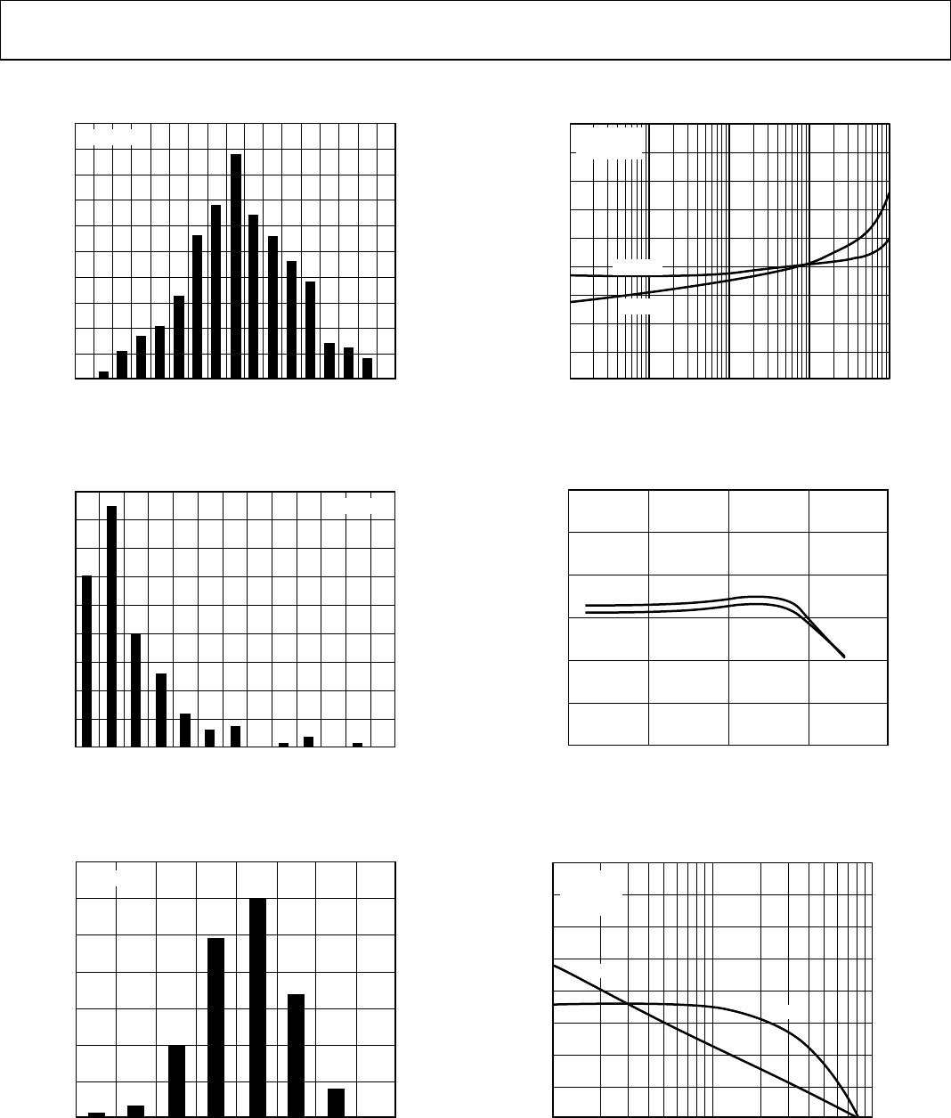
Figure 7. Input Offset Voltage Distribution
INPUT OFFSET VOLTAGE DRIFT (µV/°C)
NUMBER OF AMPLIFIERS
80
70
60
50
40
30
20
10
0.15 0.25 0.35 0.45 0.55 0.65
0
90
0.05
V
SY
= ±15V
02627-008
Figure 8. Input Offset Voltage Drift Distribution
INPUT BIAS CURRENT (nA)
NUMBER OF AMPLIFIERS
120
100
80
60
40
20
0.1 0.2 0.3 0.4 0.5 0.6 0.7
0
140
0
V
SY
= ±15V
02627-009
Figure 9. Input Bias Current Distribution
LOAD CURRENT (mA)
ΔOUTPUT VOLTAGE (V)
0.01 0.1 1
1.6
1.4
1.2
1.0
0.8
0.6
0.4
0.2
0
1.8
0.001 10
SOURCE
SINK
V
SY
= ±15V
T
A
= 25°C
02627-010
Figure 10. Output Voltage to Supply Rail vs. Load Current
TEMPERATURE (°C)
V
SY
= ±15V
INPUT BIAS CURRENT (nA)
2
1
0
–1
–2
0 50 100
3
–3
–50 150
0
2627-011
Figure 11. Input Bias Current vs. Temperature
FREQUENCY (Hz)
PHASE SHIFT (Degrees)
OPEN-LOOP GAIN (dB)
1M
50
40
30
20
10
0
–10
60
–20
100k 10M
225
180
135
90
45
0
–45
270
–90
GAIN
PHASE
V
SY
= ±15V
C
L
= 0
R
L
=
02627-012
Figure 12. Open-Loop Gain and Phase Shift vs. Frequency

OP1177ARZ-REEL7

Mfr. #:
Manufacturer:
Analog Devices Inc.
Description:
Precision Amplifiers Low Noise Low Input Bias Current SGL IC
Lifecycle:
New from this manufacturer.
Delivery:
DHL FedEx Ups TNT EMS
Payment:
T/T Paypal Visa MoneyGram Western Union