AD7741YR-REEL7

REV. 0
Information furnished by Analog Devices is believed to be accurate and
reliable. However, no responsibility is assumed by Analog Devices for its
use, nor for any infringements of patents or other rights of third parties
which may result from its use. No license is granted by implication or
otherwise under any patent or patent rights of Analog Devices.
a
AD7741/AD7742
One Technology Way, P.O. Box 9106, Norwood, MA 02062-9106, U.S.A.
Tel: 781/329-4700 World Wide Web Site: http://www.analog.com
Fax: 781/326-8703 © Analog Devices, Inc., 1999
Single and Multichannel, Synchronous
Voltage-to-Frequency Converters
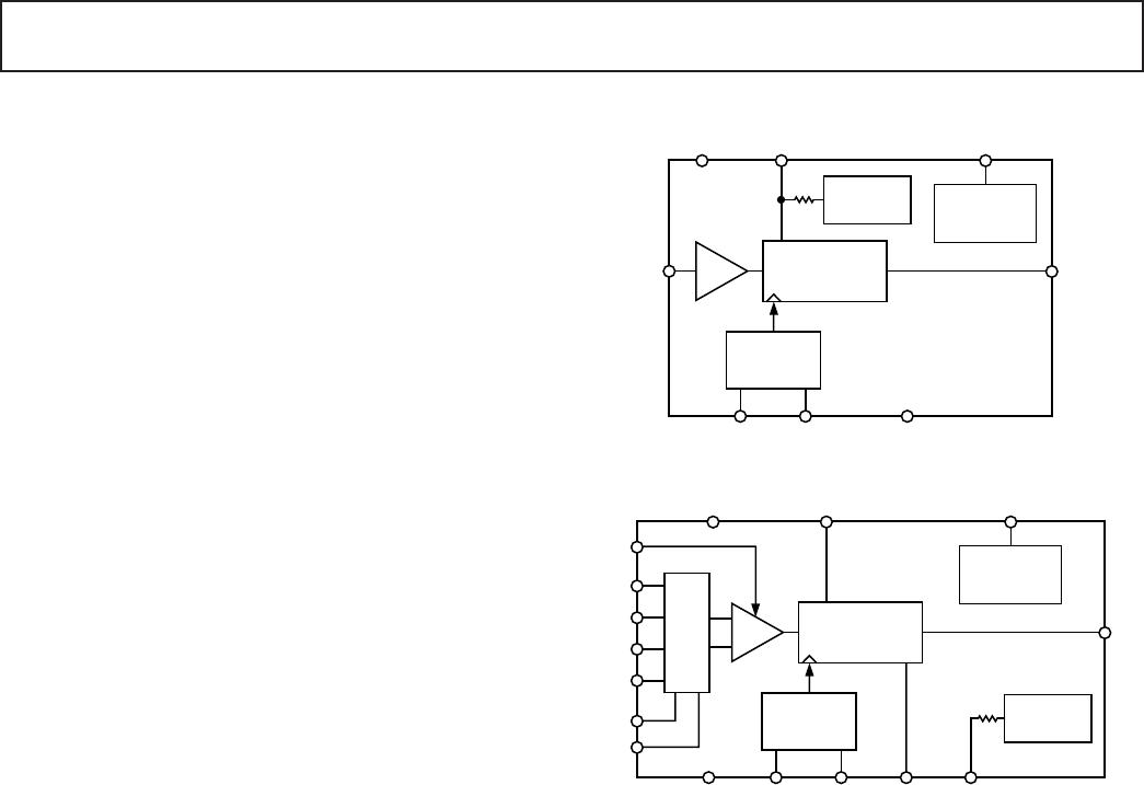
FUNCTIONAL BLOCK DIAGRAMS
X1
VOLTAGE-TO-
FREQUENCY
MODULATOR
CLOCK
GENERATION
CLKIN CLKOUT
GND
V
IN
POWER-DOWN
LOGIC
PDREFIN/OUT
V
DD
f
OUT
AD7741
+2.5V
REFERENCE
X1/X2
INPUT
MUX
VOLTAGE-TO-
FREQUENCY
MODULATOR
REFIN
+2.5V
REFERENCE
REFOUT
CLOCK
GENERATION
CLKIN CLKOUT
GND
GAIN
V
IN
1
A1
A0
V
IN
2
V
IN
3
V
IN
4
POWER-DOWN
LOGIC
PDUNI/BIP
V
DD
f
OUT
AD7742
FEATURES
AD7741: One Single-Ended Input Channel
AD7742: Two Differential or Three Pseudo-Differential
Input Channels
Integral Nonlinearity of 0.012% at f
OUT
(Max) = 2.75 MHz
(AD7742) and at f
OUT
(Max) = 1.35 MHz (AD7741)
Single +5 V Supply Operation
Buffered Inputs
Programmable Gain Analog Front-End
On-Chip +2.5 V Reference
Internal/External Reference Option
Power Down to 35 A Max
Minimal External Components Required
8-Lead and 16-Lead DIP and SOIC Packages
APPLICATIONS
Low Cost Analog-to-Digital Conversion
Signal Isolation
GENERAL DESCRIPTION
The AD7741/AD7742 are a new generation of synchronous
voltage-to-frequency converters (VFCs). The AD7741 is a
single-channel version in an 8-lead package (SOIC/DIP) and the
AD7742 is a multichannel version in a 16-lead package (SOIC/
DIP). No user trimming is required to achieve the specified
performance.
The AD7741 has a single buffered input whereas the AD7742
has four buffered inputs that may be configured as two fully-
differential inputs or three pseudo-differential inputs. Both parts
include an on-chip +2.5 V bandgap reference that provides the
user with the option of using this internal reference or an exter-
nal reference.
The AD7741 has a single-ended voltage input range from 0 V
to REFIN. The AD7742 has a differential voltage input range
from –V
REF
to +V
REF
. Both parts operate from a single +5 V
supply consuming typically 6 mA, and also contain a power-
down feature that reduces the current consumption to less than
35 µA.
REV. 0
–2–
AD7741–SPECIFICATIONS
(V
DD
= +4.75 V to +5.25 V; V
REF
= +2.5 V; f
CLKIN
= 6.144 MHz; all specifications T
MIN
to
T
MAX
unless otherwise noted.)
B and Y Version
1
Parameter
2
Min Typ Max Units Conditions/Comments
DC PERFORMANCE
Integral Nonlinearity
f
CLKIN
= 200 kHz
3
±0.012 % of Span
4
f
CLKIN
= 3 MHz
3
±0.012 % of Span
f
CLKIN
= 6.144 MHz ±0.024 % of Span V
DD
> 4.8 V
Offset Error ±40 mV
Gain Error 0 +0.8 +1.6 % of Span
Offset Error Drift
3
±30 µV/°C
Gain Error Drift
3
±16 ppm of Span/°C
Power Supply Rejection Ratio
3
–63 dB V
DD
= ±5%
ANALOG INPUT
5
Input Current ±50 ±100 nA
Input Voltage Range 0 V
REF
V
+2.5 V REFERENCE (REFIN/OUT)
REFIN
Nominal Input Voltage 2.5 V
Input Impedance
6
N/A
REFOUT
Output Voltage 2.38 2.50 2.60 V
Output Impedance
3
1k
Reference Drift
3
±50 ppm/°C
Line Rejection –60 dB
Reference Noise (0.1 Hz to 10 Hz)
3
100 µV p-p
LOGIC OUTPUT
Output High Voltage, V
OH
4.0 V Output Sourcing 800 µA
7
Output Low Voltage, V
OL
0.4 V Output Sinking 1.6 mA
7
Minimum Output Frequency 0.05 f
CLKIN
Hz V
IN
= 0 V
Maximum Output Frequency 0.45 f
CLKIN
Hz V
IN
= V
REF
LOGIC INPUT
PD ONLY
Input High Voltage, V
IH
2.4 V
Input Low Voltage, V
IL
0.8 V
Input Current ±100 nA
Pin Capacitance 6 10 pF
CLKIN ONLY
Input High Voltage, V
IH
3.5 V
Input Low Voltage, V
IL
0.8 V
Input Current ±2 µA
Pin Capacitance 6 10 pF
CLOCK FREQUENCY
Input Frequency 6.144 MHz For Specified Performance
POWER REQUIREMENTS
V
DD
4.75 5.25 V
I
DD
(Normal Mode) 8 mA Output Unloaded
I
DD
(Power-Down) 15 35 µA
Power-Up Time
3
30 µs Coming Out of Power-Down Mode
NOTES
1
Temperature ranges: B Version –40°C to +85°C: Y Version: –40°C to +105°C.
2
See Terminology.
3
Guaranteed by design and characterization, not production tested.
4
Span = Maximum Output Frequency–Minimum Output Frequency.
5
The absolute voltage on the input pin must not go more positive than V
DD
– 2.25 V or more negative than GND.
6
Because this pin is bidirectional, any external reference must be capable of sinking/sourcing 400 µA in order to overdrive the internal reference.
7
These logic levels apply to CLKOUT only when it is loaded with one CMOS load.
Specifications subject to change without notice.
REV. 0 –3
AD7741/AD7742
(V
DD
= +4.75 V to +5.25 V; V
REF
= +2.5 V; f
CLKIN
= 6.144 MHz; all specifications T
MIN
to
T
MAX
unless otherwise noted.)
B Version
1
Y Version
2
Parameter
3
Min Typ Max Min Typ Max Units Conditions/Comments
DC PERFORMANCE
Integral Nonlinearity
f
CLKIN
= 200 kHz
4
±0.0122 ±0.015 % of Span
5
f
CLKIN
= 3 MHz
4
±0.0122 ±0.015 % of Span
f
CLKIN
= 6.144 MHz ±0.0122 ±0.015 % of Span
Offset Error ±40 ±40 mV Unipolar Mode
±40 ±40 mV Bipolar Mode
Gain Error +0.2 +1.2 +2.2 +0.2 +1.2 +2.2 % of Span Unipolar Mode
+0.2 +1.2 +2.2 +0.2 +1.2 +2.2 % of Span Bipolar Mode
Offset Error Drift
4
±12 ±12 µV/°C Unipolar Mode
±12 ±12 µV/°C Bipolar Mode
Gain Error Drift
4
±2 ±2 ppm of Span/°C Unipolar Mode
±4 ±4 ppm of Span/°C Bipolar Mode
Power Supply Rejection Ratio
4
–70 –70 dB V
DD
= ±5%
Channel-to-Channel Isolation
4
–75 –75 dB
Common-Mode Rejection –60 –78 –58 –78 dB
ANALOG INPUTS (V
IN
1–V
IN
4)
6
Input Current ±50 ±100 ±50 ±100 nA
Common-Mode Input Range +0.5 V
DD
– 1.75 +0.5 V
DD
– 1.75 V
Differential Input Range –V
REF
/Gain +V
REF
/Gain –V
REF
/Gain +V
REF
/Gain V Bipolar Mode
0+V
REF
/Gain 0 +V
REF
/Gain V Unipolar Mode
VOLTAGE REFERENCE
REFIN
Nominal Input Voltage 2.5 2.5 V
Input Impedance
4
f
CLKIN
= 3 MHz 70 70 k
f
CLKIN
= 6.144 MHz 35 35 k
REFOUT
Output Voltage 2.38 2.50 2.60 2.38 2.50 2.60 V
Output Impedance
4
11k
Reference Drift
4
±50 ±50 ppm/°C
Line Rejection –70 –70 dB
Reference Noise
(0.1 Hz to 10 Hz)
4
100 100 µV p-p
LOGIC OUTPUT
Output High Voltage, V
OH
4.0 4.0 V Output Sourcing 800 µA
7
Output Low Voltage, V
OL
0.4 0.4 V Output Sinking 1.6 mA
7
Minimum Output Frequency 0.05 f
CLKIN
0.05 f
CLKIN
Hz V
IN
= 0 V (Unipolar), V
IN
=
–V
REF
/Gain (Bipolar)
Maximum Output Frequency 0.45 f
CLKIN
0.45 f
CLKIN
Hz V
IN
= V
REF
/Gain (Unipolar
and Bipolar)
LOGIC INPUT
ALL EXCEPT CLKIN
Input High Voltage, V
IH
2.4 2.4 V
Input Low Voltage, V
IL
0.8 0.8 V
Input Current ±100 ±100 nA
Pin Capacitance 6 10 6 10 pF
CLKIN ONLY
Input High Voltage, V
IH
3.5 3.5 V
Input Low Voltage, V
IL
0.8 0.8 V
Input Current ±2 ±2 µA
Pin Capacitance 6 10 6 10 pF
CLOCK FREQUENCY
Input Frequency 6.144 6.144 MHz For Specified Performance
POWER REQUIREMENTS
V
DD
4.75 5.25 4.75 5.25 V
I
DD
(Normal Mode) 6 8 6 8 mA Output Unloaded
I
DD
(Power-Down) 25 35 25 35 µA
Power-Up Time
4
30 30 µs Coming Out of Power-
Down Mode
N
OTES
1
Temperature range: B Version: –40°C to +85°C.
2
Temperature range: Y Version: –40°C to +105°C.
3
See Terminology.
4
Guaranteed by design and characterization, not production tested.
5
Span = Maximum Output Frequency–Minimum Output Frequency.
6
The absolute voltage on the input pins must not go more positive than V
DD
– 1.75 V or more negative than +0.5 V.
7
These logic levels apply to CLKOUT only when it is loaded with one CMOS load.
Specifications subject to change without notice
.
AD7742–SPECIFICATIONS

AD7741YR-REEL7

Mfr. #:
Manufacturer:
Analog Devices Inc.
Description:
Voltage to Frequency & Frequency to Voltage Low-Cost SGL-Supply SGL-Ch Sync
Lifecycle:
New from this manufacturer.
Delivery:
DHL FedEx Ups TNT EMS
Payment:
T/T Paypal Visa MoneyGram Western Union