AD7741YR-REEL7

REV. 0
AD7741/AD7742
–10–
APPLICATIONS
The basic connection diagram for the part is shown in Figure 9.
In the connection diagram shown, the AD7742 analog inputs
are configured as fully differential, bipolar inputs with a gain of
1. A quartz crystal provides the master clock source for the part.
It may be necessary to connect capacitors (C1 and C2 in the
diagram) on the crystal to ensure that it does not oscillate at over-
tones of its fundamental operating frequency. The values of ca-
pacitors will vary depending on the manufacturer’s specifications.
CLKOUTCLKIN
REFIN
f
OUT
GND
UNI/BIP
GAIN
C1 C2
DIFF
INPUT 1
DIFF
INPUT 2
CHANNEL
SELECT
V
IN
1
V
IN
2
V
IN
3
V
IN
4
A0
A1
V
DD
PD
AD7742
+5V
REFOUT
Figure 9. Basic Connection Diagram
A/D Conversion Techniques Using the AD7741/AD7742
When used as an ADC, VFCs provide certain advantages in-
cluding accuracy, linearity and being inherently monotonic. The
AD7741/AD7742 has a true integrating input which smooths
out noise peaks.
The most popular method of using a VFC in an A/D system is
to count the output pulses of f
OUT
for a fixed gate interval (see
Figure 10). This fixed gate interval should be generated by
dividing down the clock input frequency. This ensures that any
errors due to clock jitter or clock frequency drift are eliminated.
The ratio of the f
OUT
to the clock frequency is what is important
here, not the absolute value of f
OUT
. The frequency division can
be done by a binary counter where f
CLKIN
is the CLK input.
Figure 11 shows the waveforms of f
CLKIN
, f
OUT
and the Gate
signal. A counter counts the rising edges of f
OUT
while the Gate
signal is high. Since the gate interval is not synchronized with
f
OUT
, there is a possibility of a counting inaccuracy. Depending
on f
OUT,
an error of one count may occur.
COUNTERAD7741
f
OUT
V
IN
CLOCK
GENERATOR
GATE
SIGNAL
TO
m
P
CLKIN
FREQUENCY
DIVIDER
Figure 10. A/D Conversion Using the AD7741 VFC
f
CLKIN
f
OUT
GATE
T
GATE
4096x T
CLOCK
Figure 11. Waveforms in an A/D Converter Using a VFC
The clock frequency and the gate time determine the resolution
of such an ADC. If 12-bit resolution is required and f
CLKIN
is
5 MHz (therefore, f
OUT
max is 2.25 MHz), the minimum gate
time required is calculated as follows:
N counts at Full Scale (2.25 MHz) will take
(N/2.25 × 10
6
) seconds = minimum gate time.
N is the total number of codes for a given resolution; 4096 for
12 bits
minimum gate time = (4096/2.25 × 10
6
) sec = 1.820 ms.
Since T
GATE
× f
OUT
max = number of counts at full scale, a
faster conversion with the same resolution can be performed
with a higher f
OUT
max. This high f
OUT
max (3 MHz) is a main
feature of the AD7741/AD7742.
If the output frequency is measured by counting pulses gated to
a signal which is derived from the clock, the clock stability is
unimportant and the device simply performs as a voltage-
controlled frequency divider, producing a high resolution ADC.
The inherent monotonicity of the transfer function and wide
range of input clock frequencies allows the conversion time and
resolution to be optimized for specific applications.
There is another parameter is taken into account when choosing
the length of the gate interval. Because the integration period of
the system is equal to the gate interval, any interfering signal can
be rejected by counting for an integer number of periods of the
interfering signal. For example, a gate interval of 100 ms will
give normal-mode rejection of 50 Hz and 60 Hz signals.
REV. 0
AD7741/AD7742
–11–
Isolation Applications
In addition to analog-to-digital conversion, the AD7741/AD7742
can be used in isolated analog signal transmission applications.
Due to noise, safety requirements or distance, it may be neces-
sary to isolate the AD7741/AD7742 from any controlling
circuitry. This can easily be achieved by using opto-isolators,
which will provide isolation in excess of 3 kV.
Opto-electronic coupling is a popular method of isolated signal
coupling. In this type of device, the signal is coupled from an
input LED to an output photo-transistor, with light as the con-
necting medium. This technique allows dc to be transmitted, is
extremely useful in overcoming ground loops between equip-
ment, and is applicable over a wide range of speeds and power.
The analog voltage to be transmitted is converted to a pulse
train using the VFC. An opto-isolator circuit is used to couple
this pulse train across an isolation barrier using light as the
connecting medium. The input LED of the isolator is driven
from the output of the AD7741/AD7742. At the receiver side,
the output transistor is operated in the photo-transistor mode.
The pulse train can be reconverted to an analog voltage using a
frequency-to-voltage converter; alternatively, the pulse train can
be fed into a counter to generate a digital signal.
The analog and digital sections of the AD7741/AD7742 have
been designed to allow operation from a single-ended power
source, simplifying its use with isolated power supplies.
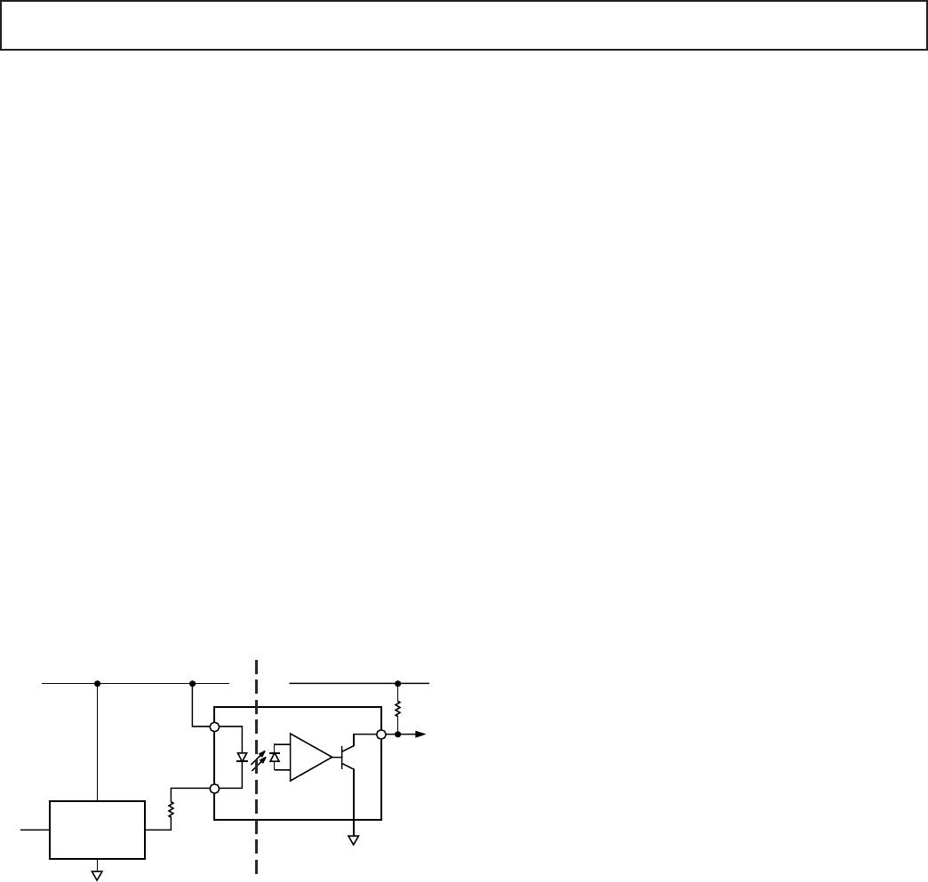
Figure 12 shows a general purpose VFC circuit using a low cost
opto-isolator. A +5 V power supply is assumed for both the
isolated (+5 V isolated) and local (+5 V local) supplies.
OPTOCOUPLER
V
CC
R
f
OUT
IN
V
DD
+5V
AD774x
GND1
GND2
ISOLATION
BARRIER
Figure 12. Opto-Isolated Application
Power Supply Bypassing and Grounding
In any circuit where accuracy is important, careful consideration
of the power supply and ground return layout helps to ensure
the rated performance. The printed circuit board housing the
AD7741/AD7742 should be designed so the analog and digital
sections are separated and confined to certain areas of the board.
To minimize capacitive coupling between them, digital and
analog ground planes should only be joined in one place, close
to the DUT and should not overlap.
Avoid running digital lines under the device as these will couple
noise onto the die. The analog ground plane should be allowed
to run under the AD7742 to avoid noise coupling. The power
supply lines to the AD7742 should use as large a trace as pos-
sible to provide low impedance paths and reduce the effects of
glitches on the power supply line. Fast switching signals like
clocks should be shielded with digital ground to avoid radiating
noise to other parts of the board and clock signals should never
be run near analog inputs. Avoid crossover of digital and analog
signals. Traces on opposite sides of the board should run at
right angles to each other. This reduces the effect of feedthrough
through the board. A microstrip technique is by far the best but
is not always possible with a double-sided board. In this tech-
nique, the component side of the board is dedicated to the ground
plane while the signal traces are placed on the solder side.
Good decoupling is also important. All analog supplies should
be decoupled to GND with surface mount capacitors, 10 µF in
parallel with 0.1 µF located as close to the package as possible,
ideally right up against the device. The lead lengths on the by-
pass capacitor should be as short as possible. It is essential that
these capacitors be placed physically close to the AD7741/AD7742
to minimize the inductance of the PCB trace between the ca-
pacitor and the supply pin. The 10 µF are the tantalum bead
type and are located in the vicinity of the VFC to reduce low-
frequency ripple. The 0.1 µF capacitors should have low Effec-
tive Series Resistance (ESR) and Effective Series Inductance
(ESI), such as the common ceramic types, which provide a low
impedance path to ground at high frequencies to handle tran-
sient currents due to internal logic switching. Additionally, it is
beneficial to have large capacitors (> 47 µF) located at the point
where the power connects to the PCB.
REV. 0
AD7741/AD7742
–12–
OUTLINE DIMENSIONS
Dimensions shown in inches and (mm).
C3601–8–5/99
PRINTED IN U.S.A.
8-Lead Plastic DIP
(N-8)
SEATING
PLANE
0.060 (1.52)
0.015 (0.38)
0.210
(5.33)
MAX
0.022 (0.558)
0.014 (0.356)
0.160 (4.06)
0.115 (2.93)
0.070 (1.77)
0.045 (1.15)
0.130
(3.30)
MIN
8
1
4
5
PIN 1
0.280 (7.11)
0.240 (6.10)
0.100 (2.54)
BSC
0.430 (10.92)
0.348 (8.84)
0.195 (4.95)
0.115 (2.93)
0.015 (0.381)
0.008 (0.204)
0.325 (8.25)
0.300 (7.62)
16-Lead Plastic DIP
(N-16)
16
18
9
PIN 1
0.840 (21.34)
0.745 (18.92)
0.280 (7.11)
0.240 (6.10)
SEATING
PLANE
0.060 (1.52)
0.015 (0.38)
0.210 (5.33)
MAX
0.022 (0.558)
0.014 (0.356)
0.160 (4.06)
0.115 (2.93)
0.100
(2.54)
BSC
0.070 (1.77)
0.045 (1.15)
0.130
(3.30)
MIN
0.195 (4.95)
0.115 (2.93)
0.015 (0.381)
0.008 (0.204)
0.325 (8.25)
0.300 (7.62)
8-Lead SO
(R-8)
0.0098 (0.25)
0.0075 (0.19)
0.0500 (1.27)
0.0160 (0.41)
0.0196 (0.50)
0.0099 (0.25)
3 458
88
08
0.102 (2.59)
0.094 (2.39)
SEATING
PLANE
0.0098 (0.25)
0.0040 (0.10)
0.0192 (0.49)
0.0138 (0.35)
85
41
0.1968 (5.00)
0.1890 (4.80)
0.2440 (6.20)
0.2284 (5.80)
PIN 1
0.1574 (4.00)
0.1497 (3.80)
0.0500 (1.27)
BSC
16-Lead Narrow Body SO
(R-16A)
16
9
8
1
0.2440 (6.20)
0.2284 (5.80)
0.1574 (4.00)
0.1497 (3.80)
PIN 1
0.3937 (10.00)
0.3859 (9.80)
0.050 (1.27)
BSC
SEATING
PLANE
0.0098 (0.25)
0.0040 (0.10)
0.0192 (0.49)
0.0138 (0.35)
0.0688 (1.75)
0.0532 (1.35)
88
08
0.0196 (0.50)
0.0099 (0.25)
3 458
0.0500 (1.27)
0.0160 (0.41)
0.0099 (0.25)
0.0075 (0.19)

AD7741YR-REEL7

Mfr. #:
Manufacturer:
Analog Devices Inc.
Description:
Voltage to Frequency & Frequency to Voltage Low-Cost SGL-Supply SGL-Ch Sync
Lifecycle:
New from this manufacturer.
Delivery:
DHL FedEx Ups TNT EMS
Payment:
T/T Paypal Visa MoneyGram Western Union