Evaluation Board for the
ADP1710/ADP1711
EVAL-ADP1710/ADP1711
Rev. 0
Evaluation boards are only intended for device evaluation and not for production purposes.
Evaluation boards as supplied “as is” and without warranties of any kind, express, implied, or
statutory including, but not limited to, any implied warranty of merchantability or fitness for a
particular purpose. No license is granted by implication or otherwise under any patents or other
intellectual property by application or use of evaluation boards. Information furnished by Analog
Devices is believed to be accurate and reliable. However, no responsibility is assumed by Analog
Devices for its use, nor for any infringements of patents or other rights of third parties that may result
from its use. Analog Devices reserves the right to change devices or specifications at any time
without notice. Trademarks and registered trademarks are the property of their respective owners.
Evaluation boards are not authorized to be used in life support devices or systems.
One Technology Way, P.O. Box 9106, Norwood, MA 02062-9106, U.S.A.
Tel: 781.329.4700 www.analog.com
Fax: 781.461.3113 ©2007 Analog Devices, Inc. All rights reserved.
FEATURES
Input voltage range: 2.5 V to 5.5 V
Output current range: 0 mA to 150 mA
Output voltage accuracy: ±1%
Operating temperature range: −40°C to +125°C
GENERAL DESCRIPTION
The ADP1710/ADP1711 evaluation boards can be used to
demonstrate the functionality of the ADP1710 and ADP1711
series of linear regulators. Depending on what component
combinations are used, the evaluation board can be used for
ADP1710 fixed output voltage devices, ADP1710 adjustable
output voltage devices, and ADP1711 fixed output voltage
devices with a bypass capacitor.
Simple device measurements such as line and load regulation,
dropout, and ground current can be demonstrated with just a
single voltage supply, a voltage meter, a current meter, and load
resistors.
For more details about the ADP1710 and ADP1711 linear
regulators, visit www.analog.com.
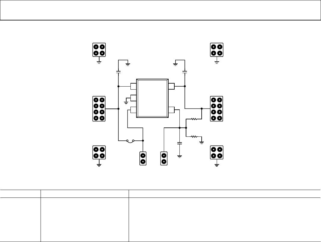
EVALUATION BOARD
GND
GND GND
GND
C1 C2
U1
C3
R1
R2
VIN VOUT
EN
J1
EVAL-ADP1710/ADP1711
NC/ADJ/BYP
NC = NO CONNECT
06311-001
Figure 1.