ADP1710-EVALZ

EVAL-ADP1710/ADP1711
Rev. 0 | Page 4 of 8
EVALUATION BOARD CONFIGURATIONS
The ADP1710/ADP1711 evaluation boards come supplied with
different components depending on which version is ordered.
Components common to all versions are C1, C2, and J1.
ADP1710 ADJUSTABLE OUTPUT
Evaluation boards that come supplied with ADP1710 adjustable
output voltage option devices have the additional R1 and R2
resistors included. Figure 3 shows the schematic of this
evaluation board configuration.
IN
GND
EN
OUT
1
2
3
5
4
ADP1710
ADJUSTABLE
U1
C1
C2
R1
R2
J1
ADJ
V
IN
V
OUT
06311-004
Figure 3. ADP1710 Adjustable Output
The output voltage is set based on the following equation:
V
OUT
= 0.8 V (1 + R1/R2)
For example, if R1 = 10 kΩ and R2 = 4.99 kΩ, then V
OUT
is 2.403 V.
ADP1711 FIXED OUTPUT WITH BYPASS
CAPACITOR
Evaluation boards that come supplied with ADP1711 fixed
output voltage option devices with a bypass capacitor have C3
populated. Figure 4 shows the schematic of this evaluation
board configuration.
IN
GND
EN
OUT
1
2
3
5
4
U1
A
DP1711
C1
C2
J1
C3
BYP
V
IN
V
OUT
06311-005
Figure 4. ADP1711 Fixed Output with Bypass Capacitor
EVAL-ADP1710/ADP1711
Rev. 0 | Page 5 of 8
OUTPUT VOLTAGE MEASUREMENTS
GND
GND GND
GND
C1 C2
U1
C3
R1
R2
VIN VOUT
EN
J1
EVAL-ADP1710/ADP1711
NC/ADJ/BYP
+
_
VOLTAGE SOURCE
+
_
VOLTMETER
V
LOAD
NC = NO CONNECT
06311-006
Figure 5.
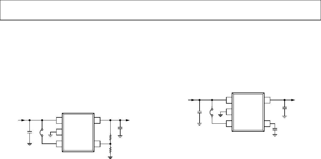
Figure 5 shows how the evaluation board can be connected to a
voltage source and a voltage meter for some basic output voltage
accuracy measurements. A resistor can be used as the load for
the regulator. Ensure the resistor has a power rating adequate
to handle the power expected to be dissipated across it. An elec-
tronic load can be used as an alternative. Ensure the voltage source
used can supply adequate current for the expected load levels.
Follow these steps to connect to a voltage source and voltage meter:
1. Connect the negative terminal (−) of the voltage source to
one of the GND pads on the evaluation board.
2. Connect the positive terminal (+) of the voltage source to
the VIN pad of the evaluation board.
3. Connect a load between the VOUT pad and one of the
GND pads.
4. Connect the negative terminal (−) of the voltage meter to
one of the GND pads, and the positive terminal (+) of the
voltage meter to the VOUT pad.
5. The voltage source can now be turned on. If J1 is inserted
(this connects EN to VIN for automatic startup), then the
regulator powers up.
If large load currents are used, then the user must connect the
voltage meter as close as possible to the output capacitor to
reduce the effects of IR drops.
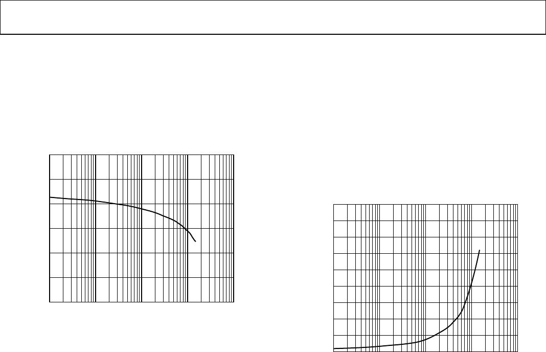
LINE REGULATION
For line regulation measurements, the regulator’s output is
monitored while its input is varied. For good line regulation,
the output must change as little as possible with varying input
levels. To ensure the device is not in dropout during this
measurement, VIN must be varied between VOUT
NOM
+ 0.5 V
(or 2.5 V, whichever is greater) to VIN
MAX
. For an ADP1710
with 3.3 V output, this means VIN needs to be varied between
3.8 V and 5.5 V. This measurement can be repeated under
different load conditions. Figure 6 shows the typical line
regulation performance of an ADP1710 with 3.3 V output.
3.32
3.26
3.3 3.8 4.3 4.8 5.3
V
IN
(V)
V
OUT
(V)
3.31
3.30
3.29
3.28
3.27
I
LOAD
= 150mA
I
LOAD
= 100mA
I
LOAD
= 50mA
I
LOAD
= 10mAI
LOAD
= 1mAI
LOAD
= 100µA
06311-007
Figure 6. ADP1710 Line Regulation
EVAL-ADP1710/ADP1711
Rev. 0 | Page 6 of 8
LOAD REGULATION
For load regulation measurements, the regulator’s output is
monitored while the load is varied. For good load regulation,
the output must change as little as possible with varying load
levels. The input voltage must be held constant during this
measurement. The load current can be varied from 0 mA to
150 mA. Figure 7 shows the typical load regulation performance
of an ADP1710 with 3.3 V output for an input voltage of 3.8 V.
3.32
3.26
0.1 1000
I
LOAD
(mA)
V
OUT
(V)
1 10 100
3.31
3.30
3.29
3.28
3.27
06311-008
Figure 7. ADP1710 Load Regulation
DROPOUT VOLTAGE
Dropout voltage measurements can also be performed using
the configuration shown in Figure 5. Dropout voltage is defined
as the input-to-output voltage differential when the input
voltage is set to the nominal output voltage. This applies only
for output voltages above 2.5 V. Dropout voltage increases with
larger loads. For more accurate measurements, a second voltage
meter can be used to monitor the input voltage across the input
capacitor. The input supply voltage may need to be adjusted to
account for IR drops, especially if large load currents are used.
Figure 8 shows a typical curve of dropout voltage measurements
with different load currents.
180
0
0.1 1000
I
LOAD
(mA)
V
DROPOUT
(mV)
1 10 100
160
140
120
100
80
60
40
20
06311-009
Figure 8. Dropout Voltage vs. Load Current

ADP1710-EVALZ

Mfr. #:
Manufacturer:
Analog Devices Inc.
Description:
ADP1710 Linear Regulator Evaluation Board
Lifecycle:
New from this manufacturer.
Delivery:
DHL FedEx Ups TNT EMS
Payment:
T/T Paypal Visa MoneyGram Western Union

Products related to this Datasheet