1
®
FN8222.3
CAUTION: These devices are sensitive to electrostatic discharge; follow proper IC Handling Procedures.
1-888-INTERSIL or 1-888-468-3774
| Intersil (and design) is a registered trademark of Intersil Americas Inc.
XDCP is a trademark of Intersil Americas Inc. Copyright Intersil Americas Inc. 2005, 2006, 2009. All Rights Reserved
All other trademarks mentioned are the property of their respective owners.
X9C102, X9C103, X9C104, X9C503
Digitally Controlled Potentiometer
(XDCP™)
The X9C102, X9C103, X9C104, X9C503 are Intersils’
digitally controlled (XDCP) potentiometers. The device
consists of a resistor array, wiper switches, a control section,
and non-volatile memory. The wiper position is controlled by
a three-wire interface.
The potentiometer is implemented by a resistor array
composed of 99 resistive elements and a wiper switching
network. Between each element and at either end are tap
points accessible to the wiper terminal. The position of the
wiper element is controlled by the CS
, U/D, and INC inputs.
The position of the wiper can be stored in non-volatile
memory and then be recalled upon a subsequent power-up
operation.
The device can be used as a three-terminal potentiometer or
as a two-terminal variable resistor in a wide variety of
applications ranging from control to signal processing to
parameter adjustment.
Pinout
X9C102, X9C103, X9C104, X9C503
(8 LD SOIC, 8 LD PDIP)
TOP VIEW
Features
Solid-State Potentiometer
Three-Wire Serial Interface
100 Wiper Tap Points
- Wiper Position Stored in Non-volatile Memory and
Recalled on Power-up
99 Resistive Elements
- Temperature Compensated
- End-to-End Resistance, ±20%
- Terminal Voltages, ±5V
Low Power CMOS
-V
CC
= 5V
- Active Current, 3mA max.
- Standby Current, 750µA max.
High Reliability
- Endurance, 100,000 Data Changes per Bit
- Register Data Retention, 100 years
X9C102 = 1kΩ
X9C103 = 10kΩ
X9C503 = 50kΩ
X9C104 = 100kΩ
Packages
- 8 Ld SOIC
- 8 Ld PDIP
Pb-Free Available (RoHS Compliant)
Block Diagram
V
CC
CS
V
L
/R
L
V
W
/R
W
INC
U/D
V
H
/R
H
V
SS
1
2
3
4
8
7
6
5
7-BIT
UP/DOWN
COUNTER
7-BIT
NON-VOLATILE
MEMORY
STORE AND
RECALL
CONTROL
CIRCUITRY
ONE
OF
HUNDRED
DECODER
RESISTOR
ARRAY
R
L
/V
L
R
W
/V
W
R
H/
V
H
U/D
INC
CS
TRANSFER
V
CC
ONE-
GATES
99
98
97
96
2
1
0
GND
UP/DOWN
(INC
)INCREMENT
DEVICE
(U/D
)
(CS
)
V
CC
(SUPPLY VOLTAGE)
V
SS
(GROUND)
CONTROL
AND
MEMORY
GENERAL
V
H
/R
H
R
W
/V
W
V
L
/R
L
SELECT
DETAILED
Data Sheet July 20, 2009
2
FN8222.3
July 20, 2009
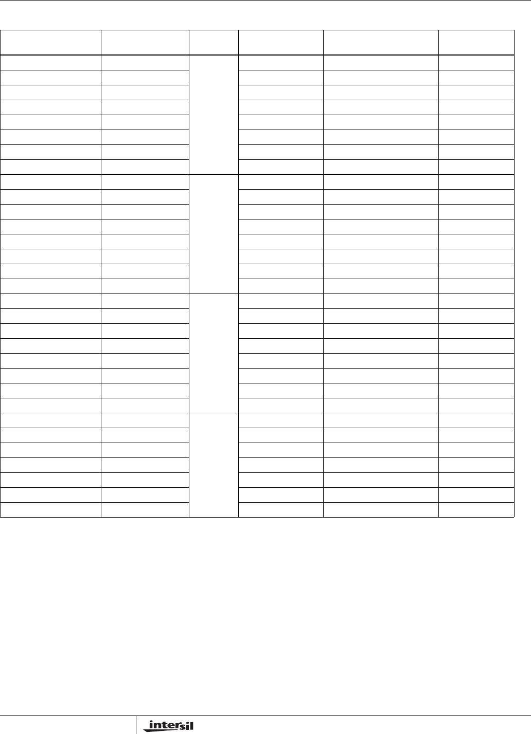
Ordering Information
PART
NUMBER
PART
MARKING
R
TOTAL
(kΩ)
TEMP RANGE
(°C) PACKAGE
PACKAGE
DWG. #
X9C102P X9C102P 1 0 to +70 8 Ld PDIP MDP0031
X9C102PZ (Notes 1, 2) X9C102P Z 0 to +70 8 Ld PDIP (Pb-free) MDP0031
X9C102PI X9C102P I -40 to +85 8 Ld PDIP MDP0031
X9C102PIZ (Notes 1, 2) X9C102P ZI -40 to +85 8 Ld PDIP (Pb-free) MDP0031
X9C102S*
,
** X9C102S 0 to +70 8 Ld SOIC MDP0027
X9C102SZ* (Note 1) X9C102S Z 0 to +70 8 Ld SOIC (Pb-free) MDP0027
X9C102SI*
,
** X9C102S I -40 to +85 8 Ld SOIC MDP0027
X9C102SIZ*
,
** (Note 1) X9C102S ZI -40 to +85 8 Ld SOIC (Pb-free) MDP0027
X9C103P X9C103P 10 0 to +70 8 Ld PDIP MDP0031
X9C103PZ (Notes 1, 2) X9C103P Z 0 to +70 8 Ld PDIP (Pb-free) MDP0031
X9C103PI X9C103P I -40 to +85 8 Ld PDIP MDP0031
X9C103PIZ (Note 1) X9C103P ZI -40 to +85 8 Ld PDIP (Pb-free) MDP0031
X9C103S*
,
** X9C103S 0 to +70 8 Ld SOIC MDP0027
X9C103SZ*
,
** (Note 1) X9C103S Z 0 to +70 8 Ld SOIC (Pb-free) MDP0027
X9C103SI*
,
** X9C103S I -40 to +85 8 Ld SOIC MDP0027
X9C103SIZ*
,
** (Note 1) X9C103S ZI -40 to +85 8 Ld SOIC (Pb-free) MDP0027
X9C503P X9C503P 50 0 to +70 8 Ld PDIP MDP0031
X9C503PZ (Notes 1, 2) X9C503P Z 0 to +70 8 Ld PDIP (Pb-free) MDP0031
X9C503PI X9C503P I -40 to +85 8 Ld PDIP MDP0031
X9C503PIZ (Notes 1, 2) X9C503P ZI -40 to +85 8 Ld PDIP (Pb-free) MDP0031
X9C503S* X9C503S 0 to +70 8 Ld SOIC MDP0027
X9C503SZ* (Note 1) X9C503S Z 0 to +70 8 Ld SOIC (Pb-free) MDP0027
X9C503SI*
,
** X9C503S I -40 to +85 8 Ld SOIC MDP0027
X9C503SIZ*
,
** (Note 1) X9C503S ZI -40 to +85 8 Ld SOIC (Pb-free) MDP0027
X9C104P X9C104P 100 0 to +70 8 Ld PDIP MDP0031
X9C104PI X9C104P I -40 to +85 8 Ld PDIP MDP0031
X9C104PIZ (Notes 1, 2) X9C104P ZI -40 to +85 8 Ld PDIP (Pb-free) MDP0031
X9C104S*
,
** X9C104S 0 to +70 8 Ld SOIC MDP0027
X9C104SZ*
,
** (Note 1) X9C104S Z 0 to +70 8 Ld SOIC (Pb-free) MDP0027
X9C104SI*
,
** X9C104S I -40 to +85 8 Ld SOIC MDP0027
X9C104SIZ*
,
** (Note 1) X9C104S ZI -40 to +85 8 Ld SOIC (Pb-free) MDP0027
*Add “T1” suffix for tape and reel. Please refer to TB347 for details on reel specifications.
**Add “T2” suffix for tape and reel. Please refer to TB347 for details on reel specifications.
NOTES:
1. These Intersil Pb-free plastic packaged products employ special Pb-free material sets, molding compounds/die attach materials, and 100%
matte tin plate plus anneal (e3 termination finish, which is RoHS compliant and compatible with both SnPb and Pb-free soldering
operations). Intersil Pb-free products are MSL classified at Pb-free peak reflow temperatures that meet or exceed the Pb-free
requirements of IPC/JEDEC J STD-020.
2. Pb-free PDIPs can be used for through-hole wave solder processing only. They are not intended for use in Reflow solder processing applications.
X9C102, X9C103, X9C104, X9C503
3
FN8222.3
July 20, 2009
Pin Descriptions
PIN
NUMBER PIN NAME DESCRIPTION
1INC
INCREMENT The INC input is negative-edge triggered. Toggling INC will move the wiper and either increment or
decrement the counter in the direction indicated by the logic level on the U/D
input.
2U/D
UP/DOWN The U/D input controls the direction of the wiper movement and whether the counter is incremented or
decremented.
3V
H
/R
H
V
H
/R
H
The high (V
H
/R
H
) terminals of the X9C102, X9C103, X9C104, X9C503 are equivalent to the fixed terminals of
a mechanical potentiometer. The minimum voltage is -5V and the maximum is +5V. The terminology of V
H
/R
H
and V
L
/R
L
references the relative position of the terminal in relation to wiper movement direction selected by the U/D input and
not the voltage potential on the terminal.
4V
SS
V
SS
5V
W
/R
W
V
W
/R
W
V
W
/R
W
is the wiper terminal and is equivalent to the movable terminal of a mechanical potentiometer. The
position of the wiper within the array is determined by the control inputs. The wiper terminal series resistance is typically
40Ω.
6R
L
/V
L
R
L
/V
L
The low (V
L
/R
L
) terminals of the X9C102, X9C103, X9C104, X9C503 are equivalent to the fixed terminals of a
mechanical potentiometer. The minimum voltage is -5V and the maximum is +5V. The terminology of V
H
/R
H
and V
L
/R
L
references the relative position of the terminal in relation to wiper movement direction selected by the U/D
input and
not the voltage potential on the terminal.
7CS
CS The device is selected when the CS input is LOW. The current counter value is stored in non-volatile memory when
CS
is returned HIGH while the INC input is also HIGH. After the store operation is complete the X9C102, X9C103,
X9C104, X9C503 device will be placed in the low power standby mode until the device is selected once again.
8V
CC
V
CC
X9C102, X9C103, X9C104, X9C503

X9C503SIZT1

Mfr. #:
Manufacturer:
Renesas / Intersil
Description:
Digital Potentiometer ICs 50K EEPOTTM POT CMOS 8LD IND
Lifecycle:
New from this manufacturer.
Delivery:
DHL FedEx Ups TNT EMS
Payment:
T/T Paypal Visa MoneyGram Western Union