6
FN8222.3
July 20, 2009
AC Timing Diagram
Pin Descriptions
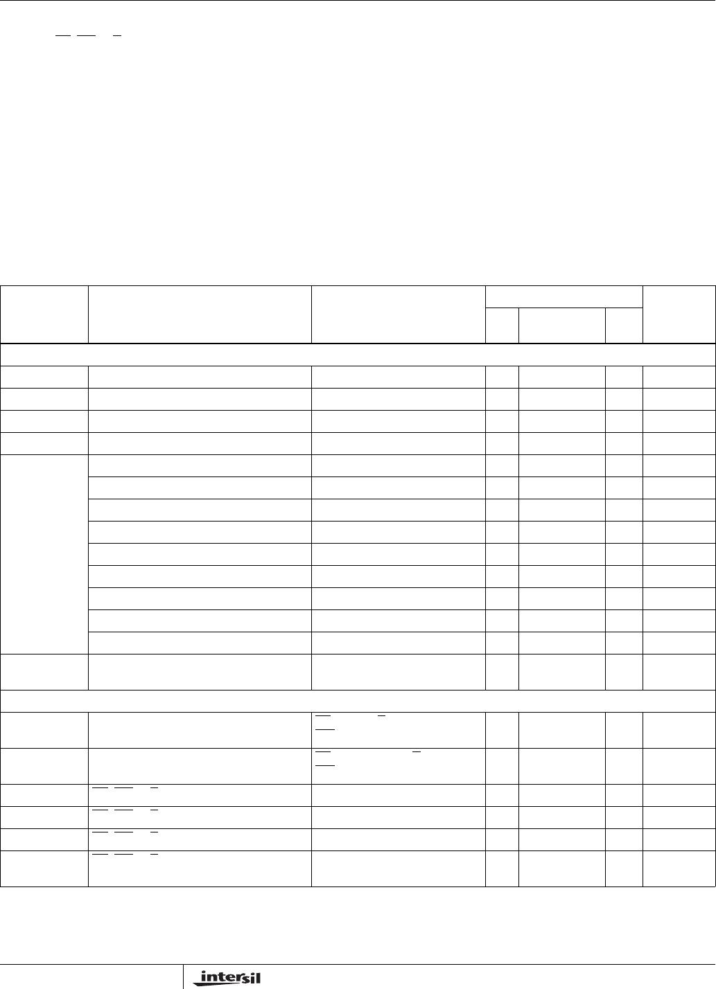
R
H
/V
H
and R
L
/V
L
The high (V
H
/R
H
) and low (V
L
/R
L
) terminals of the
ISLX9C102, X9C103, X9C104, X9C503 are equivalent to
the fixed terminals of a mechanical potentiometer. The
minimum voltage is -5V and the maximum is +5V. The
terminology of V
H
/R
H
and V
L
/R
L
references the relative
position of the terminal in relation to wiper movement
direction selected by the U/D
input and not the voltage
potential on the terminal.
R
W
/V
W
V
W
/R
W
is the wiper terminal, and is equivalent to the
movable terminal of a mechanical potentiometer. The
position of the wiper within the array is determined by the
control inputs. The wiper terminal series resistance is typically
40Ω.
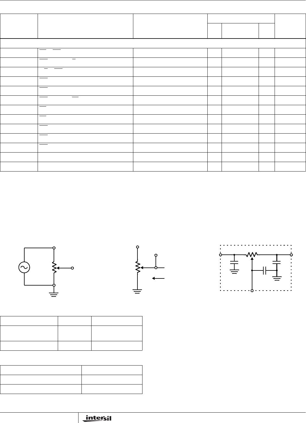
Up/Down (U/D)
The U/D input controls the direction of the wiper movement
and whether the counter is incremented or decremented.
Increment (INC)
The INC input is negative-edge triggered. Toggling INC will
move the wiper and either increment or decrement the
counter in the direction indicated by the logic level on the
U/D
input.
Chip Select (CS)
The device is selected when the CS input is LOW. The
current counter value is stored in non-volatile memory when
CS
is returned HIGH while the INC input is also HIGH. After
the store operation is complete the ISLX9C102, X9C103,
X9C104, X9C503 device will be placed in the low power
standby mode until the device is selected once again.
Principles of Operation
There are three sections of the X9C102, X9C103, ISL9C104
and ISL9C503: the input control, counter and decode section;
the non-volatile memory; and the resistor array. The input
control section operates just like an up/down counter. The
output of this counter is decoded to turn on a single electronic
switch connecting a point on the resistor array to the wiper
output. Under the proper conditions, the contents of the
counter can be stored in non-volatile memory and retained for
future use. The resistor array is comprised of 99 individual
resistors connected in series. At either end of the array and
between each resistor is an electronic switch that transfers the
potential at that point to the wiper.
The wiper, when at either fixed terminal, acts like its
mechanical equivalent and does not move beyond the last
position. That is, the counter does not wrap around when
clocked to either extreme.
The electronic switches on the device operate in a
“make-before-break” mode when the wiper changes tap
positions. If the wiper is moved several positions, multiple
taps are connected to the wiper for t
IW
(INC to V
W
/R
W
change). The R
TOTAL
value for the device can temporarily be
reduced by a significant amount if the wiper is moved
several positions.
When the device is powered-down, the last wiper position
stored will be maintained in the non-volatile memory. When
power is restored, the contents of the memory are recalled
and the wiper is reset to the value last stored.
The internal charge pump allows a wide range of voltages
(from -5V to 5V) applied to XDCP terminals yet given a
convenience of single power supply. The typical charge
pump noise of 20mV at 850kHz should be taken in
consideration when designing an application circuit.
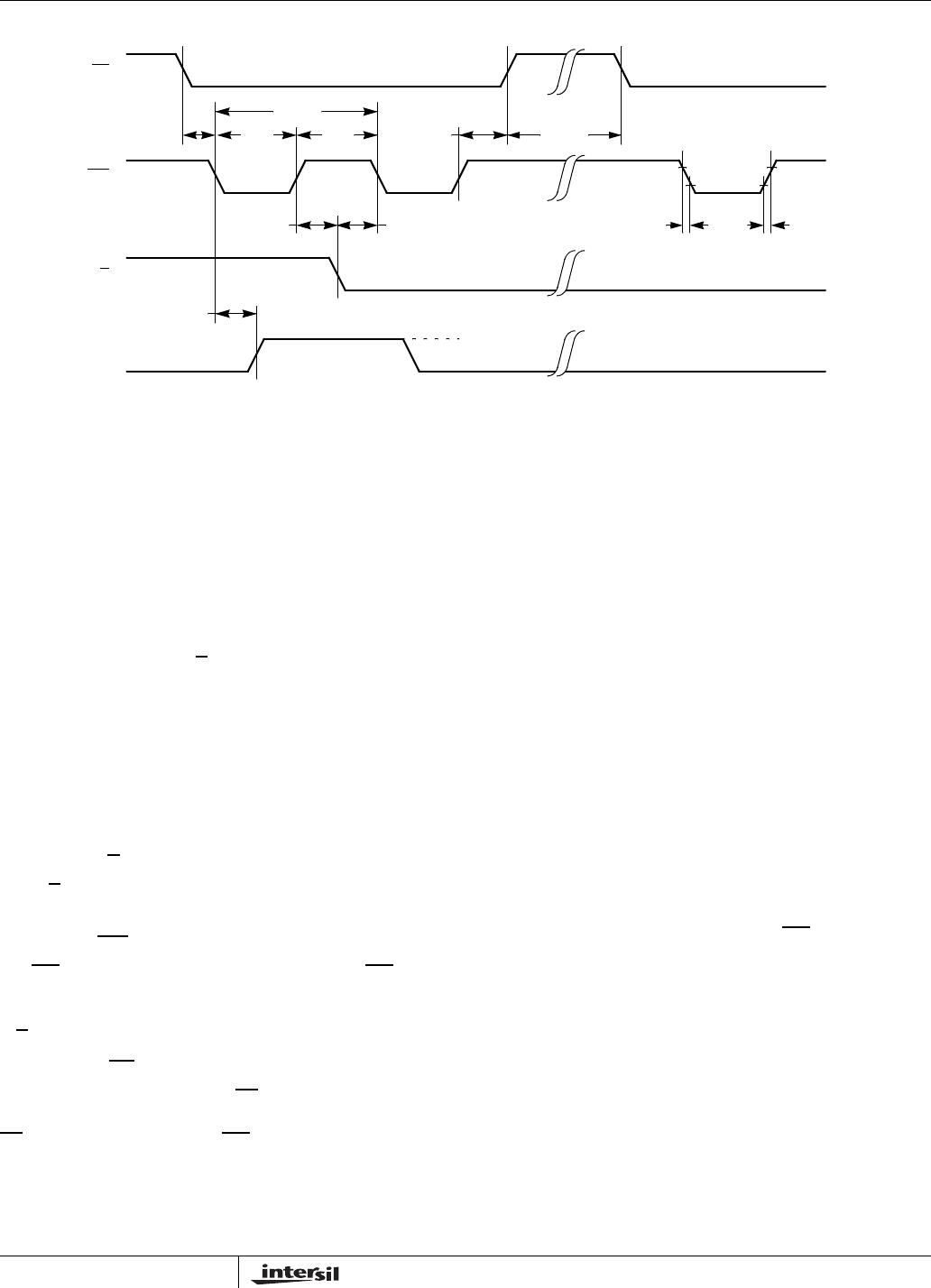
CS
INC
U/D
V
W
t
CI
t
IL
t
IH
t
CYC
t
ID
t
DI
t
IW
MI
t
IC
t
CPH
t
F
t
R
10%
90% 90%
(NOTE)
NOTE: MI REFERS TO THE MINIMUM INCREMENTAL CHANGE IN THE V
W
OUTPUT DUE TO A CHANGE IN THE WIPER POSITION.
X9C102, X9C103, X9C104, X9C503