Data Sheet ADF4106
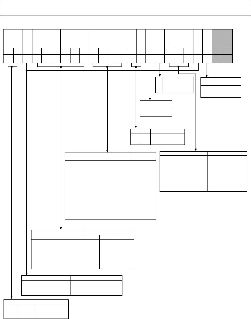
THE FUNCTION LATCH
With C2 and C1 set to 1 and 0, respectively, the on-chip
function latch is programmed. Table 9 shows the input data
format for programming the function latch.
Counter Reset
DB2 (F1) is the counter reset bit. When this is 1, the R counter
and the N (A, B) counter are reset. For normal operation, this
bit should be 0. When powering up, disable the F1 bit (set to 0).
The N counter will then resume counting in close alignment
with the R counter. (The maximum error is one prescaler cycle).
Power-Down
DB3 (PD1) and DB21 (PD2) provide programmable power-
down modes. They are enabled by the CE pin.
When the CE pin is low, the device is immediately disabled
regardless of the states of PD2, PD1.
In the programmed asynchronous power-down, the device
powers down immediately after latching 1 into the PD1 bit,
with the condition that PD2 is loaded with 0.
In the programmed synchronous power-down, the device
power-down is gated by the charge pump to prevent unwanted
frequency jumps. Once the power-down is enabled by writing 1
into the PD1 bit (provided that 1 has also been loaded to PD2),
then the device goes into power-down during the next charge
pump event.
When a power-down is activated (either synchronous or
asynchronous mode, including CE pin activated power-down),
the following events occur:
• All active dc current paths are removed.
• The R, N, and timeout counters are forced to their load state
conditions.
• The charge pump is forced into three-state mode.
• The digital clock detect circuitry is reset.
• The RF
IN
input is debiased.
• The reference input buffer circuitry is disabled.
• The input register remains active and capable of loading and
latching data.
MUXOUT Control
The on-chip multiplexer is controlled by M3, M2, and M1 on
the ADF4106 family. Table 9 shows the truth table.
Fastlock Enable Bit
DB9 of the function latch is the fastlock enable bit. When this
bit is 1, fastlock is enabled.
Fastlock Mode Bit
DB10 of the function latch is the fastlock mode bit. When
fastlock is enabled, this bit determines which fastlock mode is
used. If the fastlock mode bit is 0, then Fastlock Mode 1 is
selected; and if the fastlock mode bit is 1, then Fastlock Mode 2
is selected.
Fastlock Mode 1
The charge pump current is switched to the contents of Current
Setting 2. The device enters fastlock when 1 is written to the CP
gain bit in the N (A, B) counter latch. The device exits fastlock
when 0 is written to the CP gain bit in the N (A, B) counter
latch.
Fastlock Mode 2
The charge pump current is switched to the contents of Current
Setting 2. The device enters fastlock when 1 is written to the CP
gain bit in the N (A, B) counter latch. The device exits fastlock
under the control of the timer counter. After the timeout
period, which is determined by the value in TC4 to TC1, the CP
gain bit in the N (A, B) counter latch is automatically reset to 0,
and the device reverts to normal mode instead of fastlock. See
Table 9 for the timeout periods.
Timer Counter Control
The user has the option of programming two charge pump
currents. The intent is that Current Setting 1 is used when the
RF output is stable and the system is in a static state. Current
Setting 2 is used when the system is dynamic and in a state of
change (that is, when a new output frequency is programmed).
The normal sequence of events follows.
The user initially decides what the preferred charge pump
currents are going to be. For example, the choice may be
2.5 mA as Current Setting 1 and 5 mA as the Current Setting 2.
Simultaneously, the decision must be made as to how long the
secondary current stays active before reverting to the primary
current. This is controlled by the timer counter control bits,
DB14 to DB11 (TC4 to TC1), in the function latch. The truth
table is given in Table 9.
To program a new output frequency, simply program the N (A,
B) counter latch with new values for A and B. Simultaneously,
the CP gain bit can be set to 1, which sets the charge pump with
the value in CPI6 to CPI4 for a period of time determined by
TC4 to TC1. When this time is up, the charge pump current
reverts to the value set by CPI3 to CPI1. At the same time, the
CP gain bit in the N (A, B) counter latch is reset to 0 and is now
ready for the next time the user wishes to change the frequency.
Note that there is an enable feature on the timer counter. It is
enabled when Fastlock Mode 2 is chosen by setting the fastlock
mode bit (DB10) in the function latch to 1.
Rev. F | Page 17 of 24