ADF4106 Data Sheet
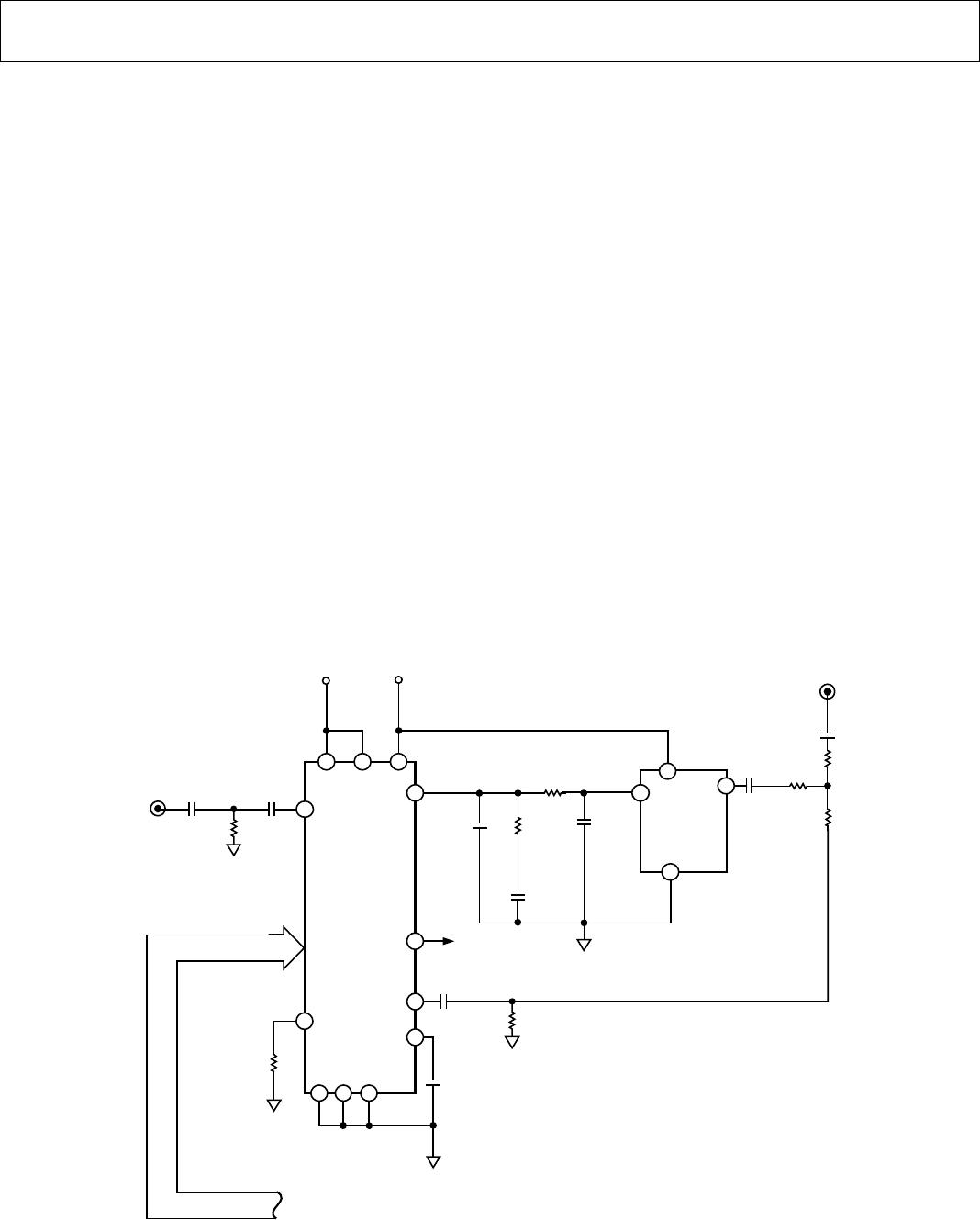
Charge Pump Currents
CPI3, CPI2, and CPI1 program Current Setting 1 for the charge
pump. CPI6, CPI5, and CPI4 program Current Setting 2 for the
charge pump. The truth table is given in Table 9.
Prescaler Value
P2 and P1 in the function latch set the prescaler values. The
prescaler value should be chosen so that the prescaler output
frequency is always less than or equal to 325 MHz. Therefore,
with an RF frequency of 4 GHz, a prescaler value of 16/17 is
valid, but a value of 8/9 is not valid.
PD Polarity
This bit sets the phase detector polarity bit. See Table 9.
CP Three-State
This bit controls the CP output pin. With the bit set high, the
CP output is put into three-state. With the bit set low, the CP
output is enabled.
THE INITIALIZATION LATCH
When C2 and C1 = 1 and 1, respectively, the initialization latch
is programmed. This is essentially the same as the function
latch (programmed when C2 and C1 = 1 and 0, respectively).
However, when the initialization latch is programmed, there is
an additional internal reset pulse applied to the R and N (A, B)
counters. This pulse ensures that the N (A, B) counter is at the
load point when the N (A, B) counter data is latched and the
device begins counting in close phase alignment.
If the latch is programmed for synchronous power-down (CE
pin is high, PD1 bit is high, and PD2 bit is low), the internal
pulse also triggers this power-down. The prescaler reference
and the oscillator input buffer are unaffected by the internal
reset pulse; therefore, close phase alignment is maintained when
counting resumes.
When the first N (A, B) counter data is latched after
initialization, the internal reset pulse is again activated.
However, successive N (A, B) counter loads after this will not
trigger the internal reset pulse.
Device Programming After Initial Power-Up
After initial power up of the device, there are three methods for
programming the device: initialization latch, CE pin, and
counter reset.
Initialization Latch Method
Apply V
DD
.
Program the initialization latch (11 in two LSBs of input
word). Make sure that the F1 bit is programmed to 0.
Do a function latch load (10 in two LSBs of the control
word), making sure that the F1 bit is programmed to a 0.
Do an R load (00 in two LSBs).
Do an N (A, B) load (01 in two LSBs).
When the initialization latch is loaded, the following occurs:
The function latch contents are loaded.
An internal pulse resets the R, N (A, B), and timeout counters
to load-state conditions and also three-states the charge
pump. Note that the prescaler band gap reference and the
oscillator input buffer are unaffected by the internal reset
pulse, allowing close phase alignment when counting
resumes.
Latching the first N (A, B) counter data after the initialization
word activates the same internal reset pulse. Successive N (A,
B) loads will not trigger the internal reset pulse, unless there
is another initialization.
CE PIN METHOD
Apply V
DD
.
Bring CE low to put the device into power-down. This is an
asychronous power-down in that it happens immediately.
Program the function latch (10).
Program the R counter latch (00).
Program the N (A, B) counter latch (01).
Bring CE high to take the device out of power-down. The R
and N (A, B) counters now resume counting in close
alignment.
Note that after CE goes high, a 1 µs duration may be required
for the prescaler band gap voltage and oscillator input buffer
bias to reach steady state.
CE can be used to power the device up and down to check for
channel activity. The input register does not need to be
reprogrammed each time the device is disabled and enabled as
long as it is programmed at least once after V
DD
is initially
applied.
COUNTER RESET METHOD
Apply V
DD
.
Do a function latch load (10 in two LSBs). As part of this,
load 1 to the F1 bit. This enables the counter reset.
Do an R counter load (00 in two LSBs).
Do an N (A, B) counter load (01 in two LSBs).
Do a function latch load (10 in two LSBs). As part of this,
load 0 to the F1 bit. This disables the counter reset.
This sequence provides the same close alignment as the
initialization method. It offers direct control over the internal
reset. Note that counter reset holds the counters at load point
and three-states the charge pump but does not trigger
synchronous power-down.
Rev. F | Page 18 of 24
Data Sheet ADF4106
APPLICATIONS
LOCAL OSCILLATOR FOR LMDS BASE STATION
TRANSMITTER
Figure 22 shows the ADF4106 being used with a VCO to
produce the LO for an LMDS base station.
The reference input signal is applied to the circuit at FREF
IN
and, in this case, is terminated in 50 Ω. A typical base station
system would have either a TCXO or an OCXO driving the
reference input without any 50 Ω termination.
To achieve a channel spacing of 1 MHz at the output, the
10 MHz reference input must be divided by 10, using the
on-chip reference divider of the ADF4106.
The charge pump output of the ADF4106 (Pin 2) drives the
loop filter. In calculating the loop filter component values, a
number of items need to be considered. In this example, the
loop filter was designed so that the overall phase margin for
the system would be 45°.
Other PLL system specifications include:
K
D
= 2.5 mA
K
V
= 80 MHz/V
Loop Bandwidth = 50 kHz
F
PFD
= 1 MHz
N = 5800
Extra Reference Spur Attenuation = 10 dB
These specifications are needed and used to derive the loop
filter component values shown in Figure 22.
The circuit in Figure 22 shows a typical phase noise
performance of −83.5 dBc/Hz at 1 kHz offset from the carrier.
Spurs are better than −62 dBc.
The loop filter output drives the VCO, which in turn is fed
back to the RF input of the PLL synthesizer and also drives the
RF output terminal. A T-circuit configuration provides 50
matching between the VCO output, the RF output, and the RF
IN
terminal of the synthesizer.
In a PLL system, it is important to know when the system
is in lock. In Figure 22, this is accomplished by using the
MUXOUT signal from the synthesizer. The MUXOUT pin
can be programmed to monitor various internal signals in the
synthesizer. One of these is the LD or lock-detect signal.
ADF4106
CE
CLK
DATA
LE
1000pF
1000pF
REF
IN
100pF
CP
MUXOUT
CPGND
AGND
DGND
100pF
1.5nF
20pF
100pF
51
6.2k
4.3k
100pF
18
NOTE
DECOUPLING CAPACITORS (0.1
µ
F/10pF) ON AV
DD
, DV
DD
, AND
V
P
OF THE ADF4106 AND ON V
CC
OF THE V956ME03 HAVE
BEEN OMITTED FROM THE DIAGRAM TO AID CLARITY.
SPI
®
-COMPATIBLE SERIAL BUS
R
SET
RF
IN
A
RF
IN
B
AV
DD
DV
DD
V
P
FREF
IN
V
DD
V
P
LOCK
DETECT
V
CC
V956ME03
1, 3, 4, 5, 7, 8,
9, 11, 12, 13
18
18
100pF
RF
OUT
5.1k
7
15
16
8
2
14
6
5
1
9
4
3
14
2
10
51
02720-027
Figure 22. Local Oscillator for LMDS Base Station
Rev. F | Page 19 of 24
ADF4106 Data Sheet
INTERFACING
The ADF4106 has a simple SPI-compatible serial interface for
writing to the device. CLK, DATA, and LE control the data
transfer. When LE goes high, the 24 bits clocked into the input
register on each rising edge of CLK are transferred to the
appropriate latch. See Figure 2 for the timing diagram and
Table 5 for the latch truth table.
The maximum allowable serial clock rate is 20 MHz. This
means that the maximum update rate for the device is 833 kHz,
or one update every 1.2 µs. This is certainly more than adequate
for systems that have typical lock times in hundreds of
microseconds.
ADuC812 Interface
Figure 23 shows the interface between the ADF4106 and the
ADuC812 MicroConverter®. Since the ADuC812 is based on an
8051 core, this interface can be used with any 8051-based
microcontroller. The MicroConverter is set up for SPI master
mode with CPHA = 0. To initiate the operation, the I/O port
driving LE is brought low. Each latch of the ADF4106 needs a
24-bit word. This is accomplished by writing three 8-bit bytes
from the MicroConverter to the device. When the third byte
is written, the LE input should be brought high to complete
the transfer.
On first applying power to the ADF4106, it needs four writes
(one each to the initialization latch, function latch, R counter
latch, and N counter latch) for the output to become active.
I/O port lines on the ADuC812 are also used to control
power-down (CE input) and to detect lock (MUXOUT
configured as lock detect and polled by the port input).
When operating in the mode described, the maximum
SCLOCK rate of the ADuC812 is 4 MHz. This means that
the maximum rate at which the output frequency can be
changed is 166 kHz.
CLK
DATA
LE
CE
MUXOUT
(LOCK DETECT)
MOSI
ADF4106
SCLOCK
I/O PORTS
ADuC812
02720-028
Figure 23. ADuC812-to-ADF4106 Interface
ADSP-2181 Interface
Figure 24 shows the interface between the ADF4106 and the
ADSP-21xx digital signal processor (DSP). The ADF4106
needs a 24-bit serial word for each latch write. The easiest way
to accomplish this using the ADSP-21xx family is to use the
autobuffered transmit mode of operation with alternate
framing. This provides a means for transmitting an entire block
of serial data before an interrupt is generated. Set up the word
length for 8 bits and use three memory locations for each 24-bit
word. To program each 24-bit latch, store the three 8-bit bytes,
enable the autobuffered mode, and write to the transmit register
of the DSP. This last operation initiates the autobuffer transfer.
CLK
DATA
LE
CE
MUXOUT
(LOCK DETECT)
MOSI
ADF4106
SCLOCK
I/O FLAGS
ADSP-21xx
TFS
02720-029
Figure 24. ADSP-21xx-to-ADF4106 Interface
PCB DESIGN GUIDELINES FOR CHIP SCALE
PACKAGE
The lands on the LFCSP (CP-20-6) are rectangular. The printed
circuit board (PCB) pad for these should be 0.1 mm longer than
the package land length and 0.05 mm wider than the package
land width. The land should be centered on the pad. This
ensures that the solder joint size is maximized. The bottom of
the LFCSP has a central thermal pad.
The thermal pad on the PCB should be at least as large as this
exposed pad. On the PCB, there should be a clearance of at least
0.25 mm between the thermal pad and the inner edges of the
pad pattern. This ensures that shorting is avoided.
Thermal vias may be used on the PCB thermal pad to improve
thermal performance of the package. If vias are used, they
should be incorporated in the thermal pad at 1.2 mm pitch grid.
The via diameter should be between 0.3 mm and 0.33 mm, and
the via barrel should be plated with 1 oz. copper to plug the via.
The user should connect the PCB thermal pad to AGND.
Rev. F | Page 20 of 24

ADF4106BRUZ-R7

Mfr. #:
Manufacturer:
Analog Devices Inc.
Description:
Phase Locked Loops - PLL Freq Synthesizer
Lifecycle:
New from this manufacturer.
Delivery:
DHL FedEx Ups TNT EMS
Payment:
T/T Paypal Visa MoneyGram Western Union