PCA9541A All information provided in this document is subject to legal disclaimers. © NXP Semiconductors N.V. 2014. All rights reserved.
Product data sheet Rev. 5 — 24 April 2014 10 of 45
NXP Semiconductors
PCA9541A
2-to-1 I
2
C-bus master selector with interrupt logic and reset
7.3.1 Register 0: Interrupt Enable (IE) register (B1:B0 = 00b)
This register allows a master to read and/or write (if needed) Mask options for its own
channel.
The Interrupt Enable register described below is identical for both the masters.
Nevertheless, there are physically 2 internal Interrupt Enable registers, one for each
upstream channel. When Master 0 reads/writes in this register, the internal Interrupt
Enable Register 0 is accessed. When Master 1 reads/writes in this register, the internal
Interrupt Enable Register 1 is accessed.
[1] Default values are the same for PCA9541A/01, PCA9541A/03.
Table 5. Register 0 - Interrupt Enable (IE) register (B1:B0 = 00b) bit allocation
7 6 5 4 3 2 1 0
0 0 0 0 BUSLOSTMSK BUSOKMSK BUSINITMSK INTINMSK
Table 6. Register 0 - Interrupt Enable (IE) register bit description
Legend: * default value
Bit Symbol Access Value
[1]
Description
7:4 - R only 0* not used
3 BUSLOSTMSK R/W 0* An interrupt on INT
will be generated after the other master has been
disconnected.
1 An interrupt on INT
will not be generated after the other master has been
disconnected.
2 BUSOKMSK R/W 0* After connection is requested and Bus Initialization not requested
(BUSINIT = 0), an interrupt on INT
will be generated when a non-idle situation
has been detected on the downstream slave channel by the bus sensor at the
switching moment.
Remark: Channel switching is done automatically after the STOP command.
1 After connection is requested and Bus Initialization not requested
(BUSINIT = 0), an interrupt on INT
will not be generated when a non-idle
situation has been detected on the downstream slave channel by the bus
sensor at the switching moment (masked).
Remark: Channel switching is done automatically after the STOP command.
1 BUSINITMSK R/W 0* After connection is requested and Bus Initialization requested (BUSINIT = 1),
an interrupt on INT
will be generated when the bus initialization is done.
Remark: Channel switching is done after bus initialization completed.
1 After connection is requested and Bus Initialization requested (BUSINIT = 1),
an interrupt on INT
will not be generated when the bus initialization is done
(masked).
Remark: Channel switching is done after bus initialization completed.
0 INTINMSK R/W 0* Interrupt on INT_IN generates an interrupt on INT.
1 Interrupt on INT_IN
does not generate an interrupt on INT (masked)
PCA9541A All information provided in this document is subject to legal disclaimers. © NXP Semiconductors N.V. 2014. All rights reserved.
Product data sheet Rev. 5 — 24 April 2014 11 of 45
NXP Semiconductors
PCA9541A
2-to-1 I
2
C-bus master selector with interrupt logic and reset
7.3.2 Register 1: Control Register (B1:B0 = 01b)
The Control Register described below is identical for both the masters. Nevertheless,
there are physically 2 internal Control Registers, one for each upstream channel.
When master 0 reads/writes in this register, the internal Control Register 0 is accessed.
When master 1 reads/writes in this register, the internal Control Register 1 is accessed.
[1] Default values are the same for PCA9541A/01, PCA9541A/03.
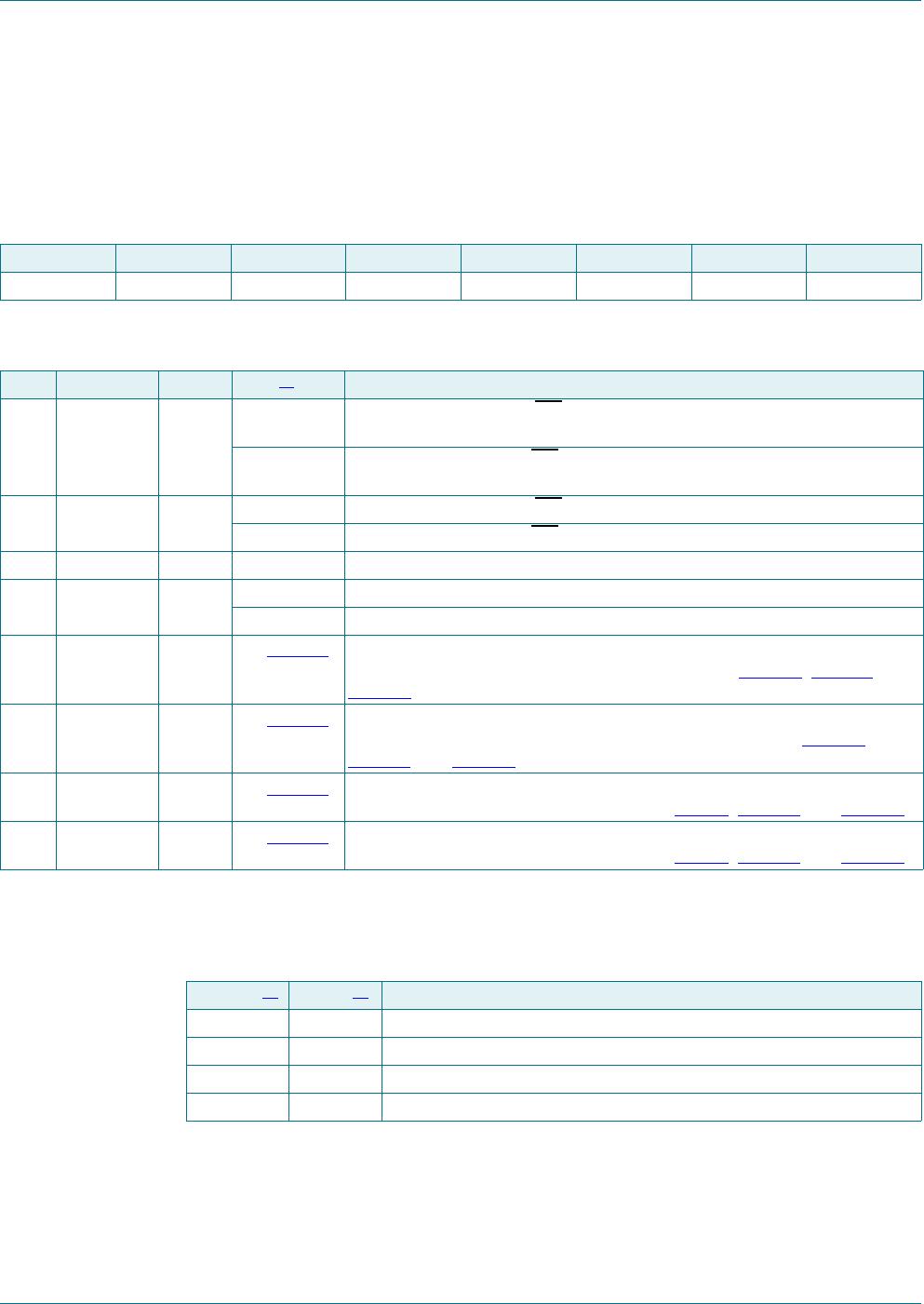
[1] MYBUS and NMYBUS is an exclusive-OR type function where:
Equal values (00b or 11b) means that the master reading its Control Register has control of the bus.
Different values (01b or 10b) means that the master reading its Control Register does not have control of
the bus.
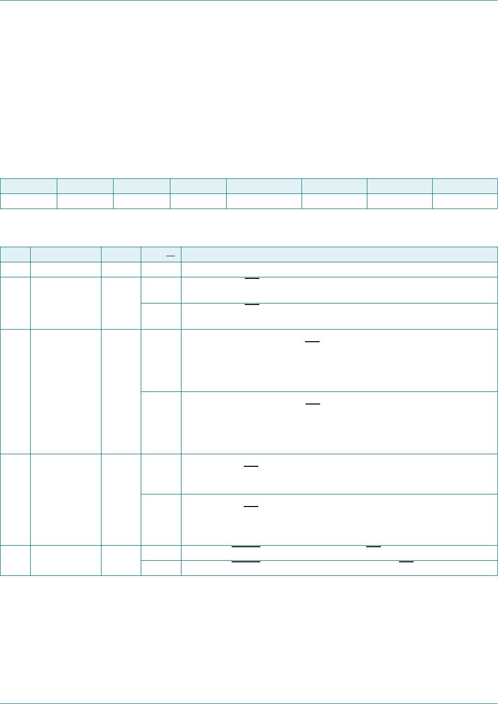
Table 7. Register 1 - Control Register (B1:B0 = 01b) bit allocation
7 6 5 4 3 2 1 0
NTESTON TESTON 0 BUSINIT NBUSON BUSON NMYBUS MYBUS
Table 8. Register 1 - Control Register (B1:B0 = 01b) bit description
Legend: * default value
Bit Symbol Access Value
[1]
Description
7 NTESTON R/W 0* A logic level HIGH to the INT
line of the other channel is sent (interrupt
cleared).
1 A logic level LOW to the INT
line of the other channel is sent (interrupt
generated).
6 TESTON R/W 0* A logic level HIGH to the INT
line is sent (interrupt cleared).
1 A logic level LOW to the INT
line is sent (interrupt generated).
5 - R only 0* not used
4 BUSINIT R/W 0* Bus initialization is not requested.
1 Bus initialization is requested.
3 NBUSON R only see Table 11
NBUSON bit along with BUSON bit decides whether any upstream channel
is connected to the downstream channel or not. See Table 10, Tab le 11, and
Table 12
.
2 BUSON R/W see Table 11
BUSON bit along with the NBUSON bit decides whether any upstream
channel is connected to the downstream channel or not. See Table 10,
Table 11, and Table 12.
1 NMYBUS R only see Table 11
NMYBUS bit along with MYBUS bit decides which upstream channel is
connected to the downstream channel. See Tab le 9
, Table 11, and Table 12.
0 MYBUS R/W see Table 11
MYBUS bit along with the NMYBUS bit decides which upstream channel is
connected to the downstream channel. See Tab le 9, Table 11, and Table 12.
Table 9. MYBUS and NMYBUS truth table
As a master reads its Control Register
NMYBUS
[1]
MYBUS
[1]
Slave channel
0 0 The master reading this combination has control of the bus.
1 0 The master reading this combination does not have control of the bus.
0 1 The master reading this combination does not have control of the bus.
1 1 The master reading this combination has control of the bus.
PCA9541A All information provided in this document is subject to legal disclaimers. © NXP Semiconductors N.V. 2014. All rights reserved.
Product data sheet Rev. 5 — 24 April 2014 12 of 45
NXP Semiconductors
PCA9541A
2-to-1 I
2
C-bus master selector with interrupt logic and reset
[1] BUSON and NBUSON is an exclusive-OR type function where:
Equal values (00b or 11b) means that the connection between the upstream and the downstream channels
is off.
Different values (01b or 10b) means that the connection between the upstream and the downstream
channels is on.
Switch to the new channel is done when the master initiating the switch request sends a
STOP command to the PCA9541A.
If either master wants to change the connection of the downstream channel, it must write
to its Control Register (Reg#01), and then send a STOP command because an update
of the connection to the downstream according to the values in the two internal Control
Registers happens only on a STOP command. Writing to one control register followed by
a STOP condition on the other master's channel does not cause an update to the
downstream connection.
When both masters request a switch to their own channel at the same time, the master
who last wrote to its Control Register before the PCA9541A receives a STOP command
wins the switching sequence. There is no arbitration performed.
The Auto Increment feature (AI = 1) allows programming the PCA9541A in 4 bytes:
Start
111A3A2A1A0 + 0 PCA9541 Address + Write
00010000 Select Reg#00 with AI = 1
Data Reg#00 Interrupt Enable Register data
Data Reg#01 Control Register data
Stop
Table 12 describes which command must be written to the Control Register when a
master device wants to take control of the I
2
C-bus. Byte written to the Control Register is
a function of the current I
2
C-bus control status performed after an initial reading of the
Control Register.
Table 10. BUSON and NBUSON truth table
NBUSON
[1]
BUSON
[1]
Slave channel
00off
10on
01on
11off
Table 11. Default Control Register values
Type version Master Bit 7 Bit 6 Bit 5 Bit 4 Bit 3 Bit 2 Bit 1 Bit 0
NTESTON TESTON not used BUSINIT NBUSON BUSON NMYBUS MYBUS
PCA9541A/01MST_000000100
MST_100001010
PCA9541A/03MST_000000000
MST_100000010

PCA9541AD/01,118

Mfr. #:
Manufacturer:
NXP Semiconductors
Description:
I/O Controller Interface IC MSTR SLCTR W/INTRPT LOGIC AND RESET
Lifecycle:
New from this manufacturer.
Delivery:
DHL FedEx Ups TNT EMS
Payment:
T/T Paypal Visa MoneyGram Western Union