NCP5030
http://onsemi.com
3
PIN FUNCTION DESCRIPTION
Pin Name Type Description
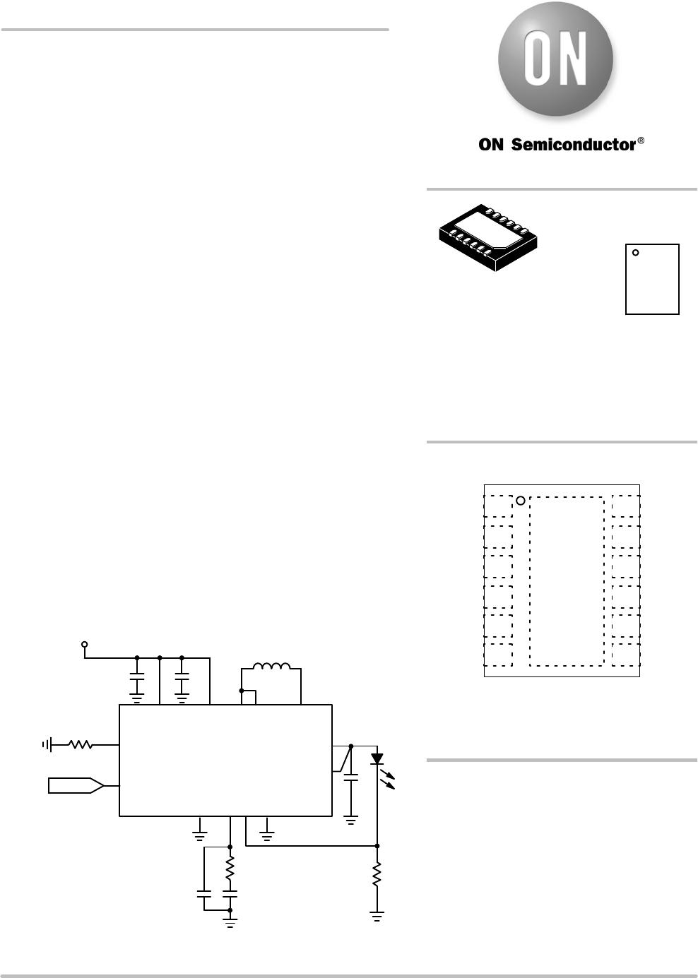
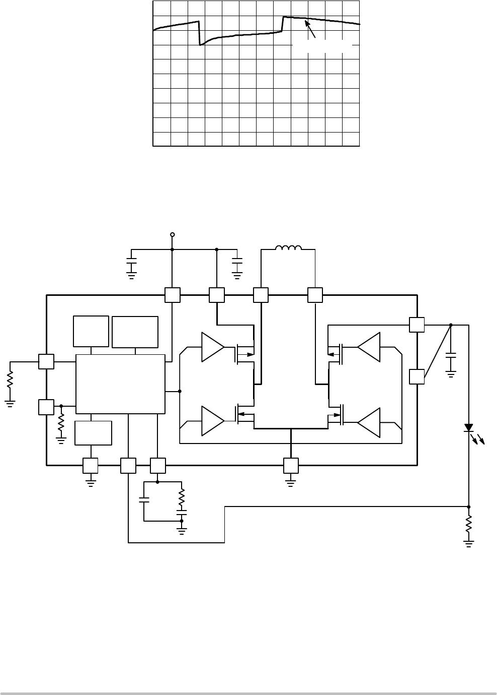
1 FB INPUT Feedback: Reference voltage is 200 mV. The cathode of the LED and a resistor to ground to set the
LED current should be connected at this point. A "5% metal film resistor, or better, is recommended
for best output accuracy. An analog signal can be applied to this input to dim the LED.
2 COMP INPUT Loop Compensation: A frequency compensation network must be connected between this pin to
the ground to ensure the stability of the closed loop. See “loop compensation” guidelines.
3 CTRL INPUT Control and Enable: An active High logic level on this pin enables the device. A built−in pulldown
resistor disables the device if the input is left open. This pin can also be used to control the average
current into the load by applying a low frequency PWM signal. If a PWM signal is applied, the
frequency should be high enough to avoid optical flicker, but be no greater than 1.0 kHz.
4 PVIN POWER Power Voltage Input Supply: A 10 mF ceramic capacitor or larger must bypass this input to the
ground. This capacitor should be placed as close a possible to this input.
5/6 LX1 POWER Switch LX1: Both pins are connected to the input node of the H−bridge. The inductor should be
connected between this node and LX2. The recommended inductor size is 4.7 mH.
7 LX2 POWER Switch LX2: This pin is connected to the opposite node of the H−bridge and the power inductor is
connected between this node and LX1.
8 VOUT POWER Power Output: A filter capacitor is necessary on this pin for the stability of the loop, to smooth the
current flowing into the load, and to limit the noise created by the fast transients present in this
circuitry. A 22 mF ceramic capacitor bypass to GND or larger is recommended. For White LED
applications, this pin is also connected to the anode of the LED. Care must be observed to avoid
EMI through the PCB copper tracks connected to this pin.
9 VS POWER Voltage Sense: This pin must be connected to C
OUT
with a dedicated track to minimize serial
parasitic inductor and to sense V
OUT
with high accuracy. This pin supplies some of the NCP5030
internal blocks when the voltage is higher than V
IN
.
10 VIN POWER Supply Pin: This pin supplies the internal control circuitry and must be connected to PVIN.
Recommended bypass capacitor is 1.0 mF ceramic or larger.
11 AGND POWER Analog Ground: This pin is the system ground and carries the analog signals. This pin must be
connected to the ground plan like PGND.
12 PCA INPUT Peak Current Adjust: A resistor between this input and ground controls the maximum peak current
allowed in the inductor. The minimum value for this resistor is 30 kW. Increasing this value decreases
the peak current. This allows the user to adjust the current based on the application needs and scale
the size of the inductor accordingly. See “Switch Current Limit“guidelines in application section.
13 PGND POWER Power Ground: This pin is the power ground for NCP5030 and carries the switching current. Care
must be observed to avoid high−density current flow in a limited PCB copper track.