CY7B991
CY7B992
Document #: 38-07138 Rev. ** Page 11 of 15
3F0 = MID, and 3F1 = High. (Since FB aligns at –4 t
U
and 3Qx
skews to +6 t
U
, a total of +10 t
U
skew is realized.) Many other con-
figurations can be realized by skewing both the output used as the
FB input and skewing the other outputs.
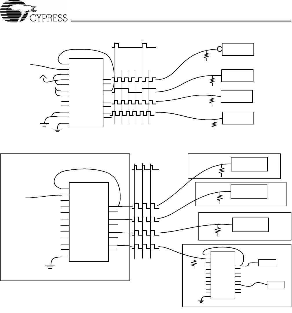
Figure 4 shows an example of the invert function of the PSCB.
In this example the 4Q0 output used as the FB input is pro-
grammed for invert (4F0 = 4F1 = HIGH) while the other three
pairs of outputs are programmed for zero skew. When 4F0 and
4F1 are tied high, 4Q0 and 4Q1 become inverted zero phase
outputs. The PLL aligns the rising edge of the FB input with the
rising edge of the REF. This causes the 1Q, 2Q, and 3Q out-
puts to become the “inverted” outputs with respect to the REF
input. By selecting which output is connect to FB, it is possible
to have 2 inverted and 6 non-inverted outputs or 6 inverted and
2 non-inverted outputs. The correct configuration would be de-
termined by the need for more (or fewer) inverted outputs. 1Q,
2Q, and 3Q outputs can also be skewed to compensate for
varying trace delays independent of inversion on 4Q.
Figure 5 illustrates the PSCB configured as a clock multiplier.
The 3Q0 output is programmed to divide by four and is fed
back to FB. This causes the PLL to increase its frequency until
the 3Q0 and 3Q1 outputs are locked at 20 MHz while the 1Qx
and 2Qx outputs run at 80 MHz. The 4Q0 and 4Q1 outputs are
programmed to divide by two, which results in a 40-MHz wave-
form at these outputs. Note that the 20- and 40-MHz clocks fall
simultaneously and are out of phase on their rising edge. This
will allow the designer to use the rising edges of the
1
⁄
2
fre-
quency and
1
⁄
4
frequency outputs without concern for ris-
ing-edge skew. The 2Q0, 2Q1, 1Q0, and 1Q1 outputs run at
80 MHz and are skewed by programming their select inputs
accordingly. Note that the FS pin is wired for 80-MHz operation
because that is the frequency of the fastest output.
Figure 6 demonstrates the PSCB in a clock divider application.
2Q0 is fed back to the FB input and programmed for zero skew.
3Qx is programmed to divide by four. 4Qx is programmed to
divide by two. Note that the falling edges of the 4Qx and 3Qx
outputs are aligned. This allows use of the rising edges of the
1
⁄
2
frequency and
1
⁄
4
frequency without concern for skew
mismatch. The 1Qx outputs are programmed to zero skew and
are aligned with the 2Qx outputs. In this example, the FS input
is grounded to configure the device in the 15- to 30-MHz range
since the highest frequency output is running at 20 MHz.
Figure 7 shows some of the functions that are selectable on
the 3Qx and 4Qx outputs. These include inverted outputs and
outputs that offer divide-by-2 and divide-by-4 timing. An invert-
ed output allows the system designer to clock different sub-
systems on opposite edges, without suffering from the pulse
asymmetry typical of non-ideal loading. This function allows
the two subsystems to each be clocked 180 degrees out of
phase, but still to be aligned within the skew spec.
The divided outputs offer a zero-delay divider for portions of
the system that need the clock to be divided by either two or
four, and still remain within a narrow skew of the “1X” clock.
Without this feature, an external divider would need to be add-
ed, and the propagation delay of the divider would add to the
skew between the different clock signals.
These divided outputs, coupled with the Phase Locked Loop,
allow the PSCB to multiply the clock rate at the REF input by
either two or four. This mode will enable the designer to dis-
tribute a low-frequency clock between various portions of the
system, and then locally multiply the clock rate to a more suit-
able frequency, while still maintaining the low-skew character-
istics of the clock driver. The PSCB can perform all of the func-
tions described above at the same time. It can multiply by two
and four or divide by two (and four) at the same time that it is
shifting its outputs over a wide range or maintaining zero skew
between selected outputs.
Figure 4. Inverted Output Connections
Figure 5. Frequency Multiplier with Skew Connections
7B991–11
FB
REF
FS
4F0
4F1
3F0
3F1
2F0
2F1
1F0
1F1
4Q0
4Q1
3Q0
3Q1
2Q0
2Q1
1Q0
1Q1
TEST
REF
7B991–12
FB
REF
FS
4F0
4F1
3F0
3F1
2F0
2F1
1F0
1F1
4Q0
4Q1
3Q0
3Q1
2Q0
2Q1
1Q0
1Q1
TEST
REF
20 MHz
20 MHz
40 MHz
80 MHz
Figure 6. Frequency Divider Connections
7B991–13
FB
REF
FS
4F0
4F1
3F0
3F1
2F0
2F1
1F0
1F1
4Q0
4Q1
3Q0
3Q1
2Q0
2Q1
1Q0
1Q1
TEST
REF
20 MHz
5 MHz
10 MHz
20 MHz