LT1678/LT1679
1
sn16789 16789fs
FEATURES
APPLICATIO S
U
DESCRIPTIO
U
TYPICAL APPLICATIO
U
Dual/Quad Low Noise,
Rail-to-Rail, Precision Op Amps
Rail-to-Rail Input and Output
100% Tested Low Voltage Noise:
3.9nV/Hz Typ at 1kHz
5.5nV/Hz Max at 1kHz
Single Supply Operation from 2.7V to 36V
Offset Voltage: 100µV Max
Low Input Bias Current: 20nA Max
High A
VOL
: 3V/µV Min, R
L
= 10k
High CMRR: 100dB Min
High PSRR: 106dB Min
Gain Bandwidth Product: 20MHz
Operating Temperature Range: –40°C to 85°C
Matching Specifications
No Phase Inversion
8-Lead SO and 14-Lead SO Packages
The LT
®
1678/LT1679 are dual/quad rail-to-rail op amps
offering both low noise and precision: 3.9nV/Hz wideband
noise, 1/f corner frequency of 4Hz and 90nV peak-to-peak
0.1Hz to 10Hz noise are combined with outstanding
precision: 100µV maximum offset voltage, greater than
100dB common mode and power supply rejection and
20MHz gain bandwidth product. The LT1678/LT1679 bring
precision as well as low noise to single supply applications as
low as 3V. The input range exceeds the power supply by
100mV with no phase inversion while the output can swing
to within 170mV of either rail.
The LT1678/LT1679 are offered in the SO-8 and SO-14
packages. A full set of matching specifications are also
provided, facilitating their use in matching dependent appli-
cations such as a two op amp instrumentation amplifier
design. The LT1678/LT1679 are specified for supply volt-
ages of ±15V, single 5V as well as single 3V. For a single
amplifier with similiar performance, see the LT1677 data
sheet.
Instrumentation Amplifier with Shield Driver
Strain Gauge Amplifiers
Portable Microphones
Battery-Powered Rail-to-Rail Instrumentation
Low Noise Signal Processing
Microvolt Accuracy Threshold Detection
Infrared Detectors
, LTC and LT are registered trademarks of Linear Technology Corporation.
0.1Hz to 10Hz Voltage Noise
+
1/4
LT1679
16789 TA01
+
+
1/4
LT1679
1/4
LT1679
15V
15V
OUTPUT
1/4
LT1679
30k1k
R
F
3.4k
R
G
100
R
F
3.4k
30k
1k
5
4
6
11
7
1
3
2
10
9
8
14
13
12
+
INPUT
GUARD
GUARD
R
G
100
+
GAIN = 1000
TIME (sec)
VOLTAGE NOISE (50nV/DIV)
16789 TA01b
V
S
= ±2.5V
4681002
LT1678/LT1679
2
sn16789 16789fs
SYMBOL PARAMETER CONDITIONS (Note 6) MIN TYP MAX UNITS
V
OS
Input Offset Voltage (Note 11) 35 100 µV
0°C T
A
70°C 55 270 µV
–40°C T
A
85°C 75 350 µV
V
S
=5V, V
CM
= V
S
+ 0.1V 150 550 µV
V
S
=5V, V
CM
= V
S
– 0.3V, 0°C T
A
70°C 180 750 µV
V
S
=5V, V
CM
= V
S
– 0.3V, –40°C T
A
85°C 200 1000 µV
V
S
=5V, V
CM
= –0.1V 1.5 30 mV
V
S
=5V, V
CM
= 0V, 0°C T
A
70°C 1.8 45 mV
V
S
=5V, V
CM
= 0V, –40°C T
A
85°C 2.0 50 mV
V
OS
Average Input Offset Drift (Note 10) 0.40 3 µV/°C
Temp
I
B
Input Bias Current (Note 11) ±2 ±20 nA
0°C T
A
70°C ±3 ±35 nA
–40°C T
A
85°C ±7 ±50 nA
V
S
= 5V, V
CM
= V
S
+ 0.1V 0.19 0.40 µA
V
S
= 5V, V
CM
= V
S
– 0.3V, 0°C T
A
70°C 0.19 0.60 µA
V
S
= 5V, V
CM
= V
S
– 0.3V, –40°C T
A
85°C 0.25 0.75 µA
V
S
= 5V, V
CM
= –0.1V 5 0.41 µA
V
S
= 5V, V
CM
= 0V, 0°C T
A
70°C 8.4 0.45 µA
V
S
= 5V, V
CM
= 0V, –40°C T
A
85°C –10 0.47 µA
The denotes the specifications which apply over the full operating
temperature range, otherwise specifications are at T
A
= 25°C. V
S
= 3V, V
CM
= V
O
= 1.7V; V
S
= 5V, V
CM
= V
O
= 2.5V unless
otherwise noted.
ELECTRICAL CHARACTERISTICS
(Note 1)
Supply Voltage ...................................................... ±18V
Input Voltages (Note 2) ............ 0.3V Beyond Either Rail
Differential Input Current (Note 2) ..................... ±25mA
Output Short-Circuit Duration (Note 3) ............ Indefinite
Storage Temperature Range ................. 65°C to 150°C
ORDER PART
NUMBER
LT1678CS8
LT1678IS8
S8 PART MARKING
1678
1678I
T
JMAX
= 150°C, θ
JA
= 190°C/ W
ABSOLUTE AXI U RATI GS
WWWU
PACKAGE/ORDER I FOR ATIO
UU
W
Consult LTC Marketing for parts specified with wider operating temperature ranges.
Lead Temperature (Soldering, 10 sec.)................. 300°C
Operating Temperature Range
(Note 4)............................................. 40°C to 85°C
Specified Temperature Range
(Note 5)............................................. 40°C to 85°C
ORDER PART
NUMBER
LT1679CS
LT1679IS
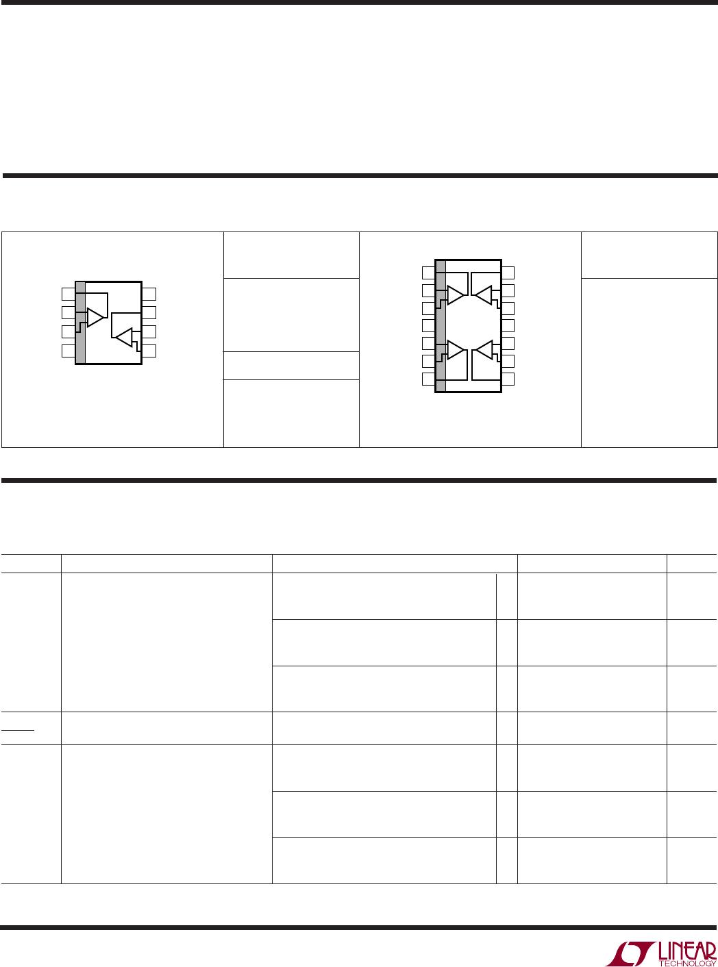
TOP VIEW
S PACKAGE
14-LEAD PLASTIC SO
1
2
3
4
5
6
7
14
13
12
11
10
9
8
OUT A
–IN A
+IN A
V
+
+IN B
–IN B
OUT B
OUT D
–IN D
+IN D
V
+IN C
–IN C
OUT C
AD
CB
T
JMAX
= 150°C, θ
JA
= 160°C/ W
TOP VIEW
S8 PACKAGE
8-LEAD PLASTIC SO
1
2
3
4
8
7
6
5
OUT A
V
+
OUT B
IN B
+IN B
IN A
+IN A
V
A
B
LT1678/LT1679
3
sn16789 16789fs
SYMBOL PARAMETER CONDITIONS (Note 6) MIN TYP MAX UNITS
I
OS
Input Offset Current (Note 11) 4 25 nA
0°C T
A
70°C 535 nA
–40°C T
A
85°C 855 nA
V
S
= 5V, V
CM
= V
S
+ 0.1V 6 30 nA
V
S
= 5V, V
CM
= V
S
– 0.3V, 0°C T
A
70°C 10 40 nA
V
S
= 5V, V
CM
= V
S
– 0.3V, –40°C T
A
85°C 15 65 nA
V
S
= 5V, V
CM
= –0.1V 0.1 1.6 µA
V
S
= 5V, V
CM
= 0V, 0°C T
A
70°C 0.1 2.0 µA
V
S
= 5V, V
CM
= 0V, –40°C T
A
85°C 0.15 2.4 µA
e
n
Input Noise Voltage 0.1Hz to 10Hz (Note 7) 90 nV
P-P
V
CM
= V
S
180 nV
P-P
V
CM
= 0V 1600 nV
P-P
Input Noise Voltage Density (Note 8) f
O
= 10Hz 4.4 nV/Hz
V
CM
= V
S
, f
O
= 10Hz 6.6 nV/Hz
V
CM
= 0V, f
O
= 10Hz 19 nV/Hz
f
O
= 1kHz 3.9 5.5 nV/Hz
V
CM
= V
S
, f
O
= 1kHz 5.3 nV/Hz
V
CM
= 0V, f
O
= 1kHz 9 nV/Hz
i
n
Input Noise Current Density f
O
= 10Hz 1.2 pA/Hz
f
O
= 1kHz 0.3 pA/Hz
V
CM
Input Voltage Range 0.1 V
S
+ 0.1V V
0V
S
– 0.3V V
R
IN
Input Resistance Common Mode 2 G
C
IN
Input Capacitance 4.2 pF
CMRR Common Mode Rejection Ratio V
S
= 5V, V
CM
= 1.9V to 3.9V 98 120 dB
V
S
= 5V, V
CM
= 1.9V to 3.9V 92 120 dB
PSRR Power Supply Rejection Ratio V
S
= 2.7V to 36V, V
CM
= V
O
= 1.7V 100 125 dB
V
S
= 3.1V to 36V, V
CM
= V
O
= 1.7V 98 120 dB
A
VOL
Large-Signal Voltage Gain V
S
= 3V, R
L
= 10k, V
O
= 2.5V to 0.7V 0.6 3 V/µV
0.3 2 V/µV
V
S
= 3V, R
L
= 2k, V
O
= 2.2V to 0.7V 0.5 3 V/µV
0°C T
A
70°C 0.4 0.9 V/µV
–40°C T
A
85°C 0.4 0.8 V/µV
V
S
= 3V, R
L
= 600, V
O
= 2.2V to 0.7V 0.20 0.43 V/µV
0°C T
A
70°C 0.15 0.40 V/µV
–40°C T
A
85°C 0.10 0.35 V/µV
V
S
= 5V, R
L
= 10k, V
O
= 4.5V to 0.7V 1 3.8 V/µV
O°C < T
A
< 70°C 0.6 2 V/µV
–40 < T
A
< 85°C 0.3 2 V/µV
V
S
= 5V, R
L
= 2k, V
O
= 4.2V to 0.7V 0.7 3.5 V/µV
0°C T
A
70°C 0.6 3.2 V/µV
–40°C T
A
85°C 0.5 3.0 V/µV
V
S
= 5V, R
L
= 600, V
O
= 4.2V to 0.7V 0.6 3.0 V/µV
0°C T
A
70°C 0.5 2.8 V/µV
–40°C T
A
85°C 0.4 2.5 V/µV
V
OL
Output Voltage Swing Low (Note 11) Above GND
I
SINK
= 0.1mA 80 170 mV
0°C T
A
70°C 125 200 mV
40°C T
A
85°C 130 250 mV
The denotes the specifications which apply over the full operating
temperature range, otherwise specifications are at T
A
= 25°C. V
S
= 3V, V
CM
= V
O
= 1.7V; V
S
= 5V, V
CM
= V
O
= 2.5V unless
otherwise noted.
ELECTRICAL CHARACTERISTICS

LT1679CS#PBF

Mfr. #:
Manufacturer:
Analog Devices Inc.
Description:
Precision Amplifiers Quad Low Noise R-to-R Pre OA
Lifecycle:
New from this manufacturer.
Delivery:
DHL FedEx Ups TNT EMS
Payment:
T/T Paypal Visa MoneyGram Western Union