LT1678/LT1679
7
sn16789 16789fs
Note 1: Absolute Maximum Ratings are those values beyond which the life
of the device may be impaired.
Note 2: The inputs are protected by back-to-back diodes. Current limiting
resistors are not used in order to achieve low noise. If differential input
voltage exceeds ±1.4V, the input current should be limited to 25mA. If the
common mode range exceeds either rail, the input current should be
limited to 10mA.
Note 3: A heat sink may be required to keep the junction temperature
below absolute maximum.
Note 4: The LT1678C/LT1679C and LT1678I/LT1679I are guaranteed
functional over the Operating Temperature Range of –40°C to 85°C.
Note 5: The LT1678C/LT1679C are guaranteed to meet specified
performance from 0°C to 70°C. The LT1678C/LT1679C are designed,
characterized and expected to meet specified performance from – 40°C to
85°C but is not tested or QA sampled at these temperatures. The LT1678I/
LT1679I are guaranteed to meet specified performance from – 40°C to
85°C.
Note 6: Typical parameters are defined as the 60% yield of parameter
distributions of individual amplifier; i.e., out of 100 LT1678/LT1679s,
typically 60 op amps will be better than the indicated specification.
Note 7: See the test circuit and frequency response curve for 0.1Hz to10Hz
tester in the Applications Information section.
Note 8: Noise is 100% tested at ±15V supplies.
Note 9: Slew rate is measured in A
V
= – 1; input signal is ±10V, output
measured at ±5V.
Note 10: This parameter is not 100% tested.
Note 11: V
S
= 5V limits are guaranteed by correlation to V
S
= 3V and
V
S
= ±15V tests.
Note 12: V
S
= 3V limits are guaranteed by correlation to V
S
= 5V and
V
S
= ±15V tests.
Note 13: Guaranteed by correlation to slew rate at V
S
= ±15V and GBW at
V
S
= 3V and V
S
= ±15V tests.
Note 14: ∆CMRR and ∆PSRR are defined as follows:
1. CMRR and PSRR are measured in µV/V on the individual amplifiers.
2. The difference is calculated between the matching sides in µV/V.
3. The result is converted to dB.
Note 15: Matching parameters are the difference between amplifiers A and
B on the LT1678 and between amplifiers A and D and B and C in the
LT1679.
Note 16: Input range guaranteed by the common mode rejection ratio test.
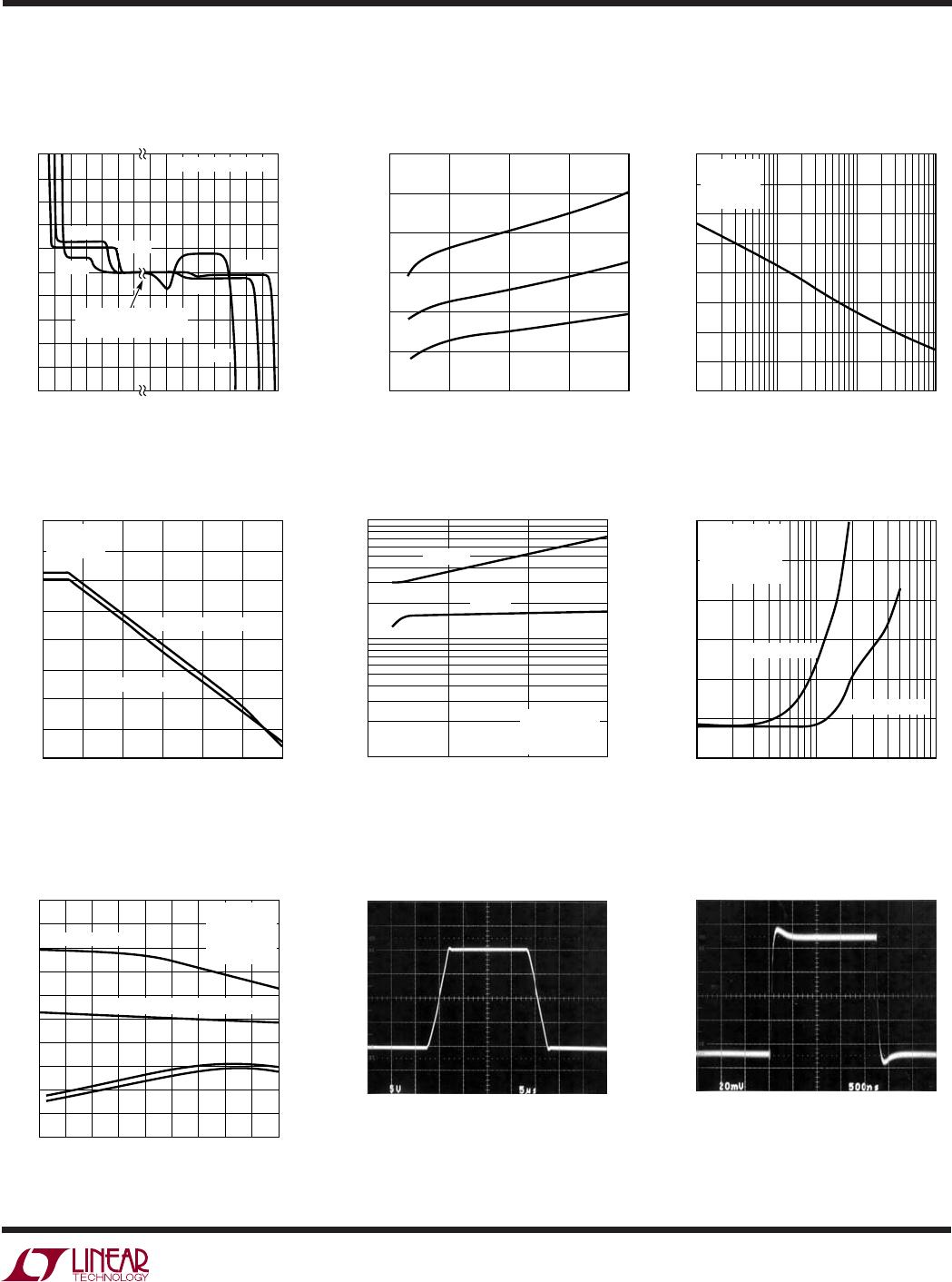
ELECTRICAL CHARACTERISTICS
TYPICAL PERFOR A CE CHARACTERISTICS
UW
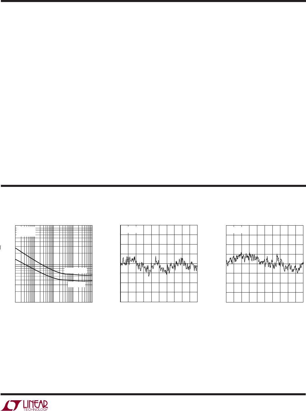
FREQUENCY (Hz)
0.1
1
NOISE VOLTAGE (nV/√Hz)
10
100
10 1000
16789 G01
1 100
16789 G02
VOLTAGE NOISE (50nV/DIV)
16789 G03
V
S
= ±15V
T
A
= 25°C
V
CM
= 0V
V
CM
= 14.5V
V
S
= 5V, 0V
TIME (sec)
VOLTAGE NOISE (50nV/DIV)
V
S
= 5V, 0V
4681002
TIME (sec)
40 60 80 100020
Voltage Noise vs Frequency
0.1Hz to 10Hz Voltage Noise
0.01Hz to 1Hz Voltage Noise