LT1678/LT1679
13
sn16789 16789fs
Rail-to-Rail Input
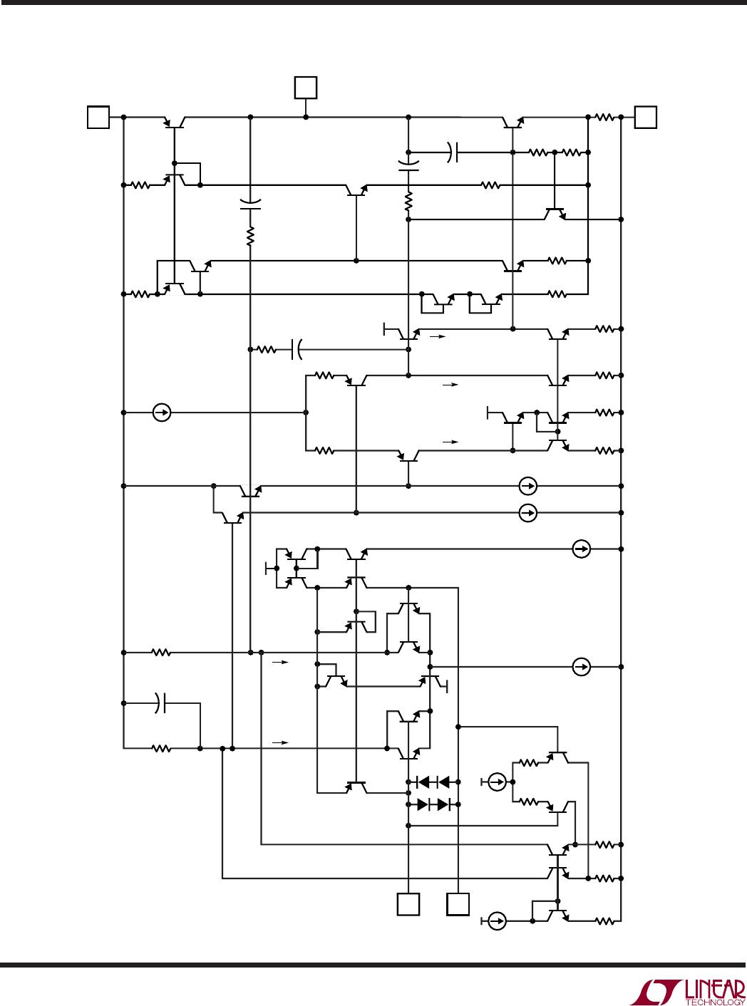
The input common mode range for the
LT1678/LT1679
can exceed the supplies by at least 100mV. As the
common mode voltage approaches the positive rail (+V
S
– 0.7V), the tail current for the input pair (Q1, Q2) is
reduced, which prevents the input pair from saturating
(refer to the Simplified Schematic). The voltage drop
across the load resistors R
C1
, R
C2
is reduced to less than
200mV, degrading the slew rate, bandwidth, voltage
noise, offset voltage and input bias current (the cancella-
tion is shut off).
When the input common mode range goes below 1.5V
above the negative rail, the NPN input pair (Q1, Q2) shuts
off and the PNP input pair (Q8, Q9) turns on. The offset
voltage, input bias current, voltage noise and bandwidth
are also degraded. The graph of Offset Voltage Shift vs
Common Mode shows where the knees occur by display-
ing the change in offset voltage. The change-over points
are temperature dependent; see the graph Common Mode
Range vs Temperature.
Rail-to-Rail Output
The rail-to-rail output swing is achieved by using transis-
tor collectors (Q28, Q29 referring to the Simplified Sche-
matic) instead of customary class A-B emitter followers for
the output stage. The output NPN transistor (Q29) sinks the
current necessary to move the output in the negative direc-
tion. The change in Q29’s base emitter voltage is reflected
directly to the gain node (collectors of Q20 and Q16). For
large sinking currents, the delta V
BE
of Q29 can dominate
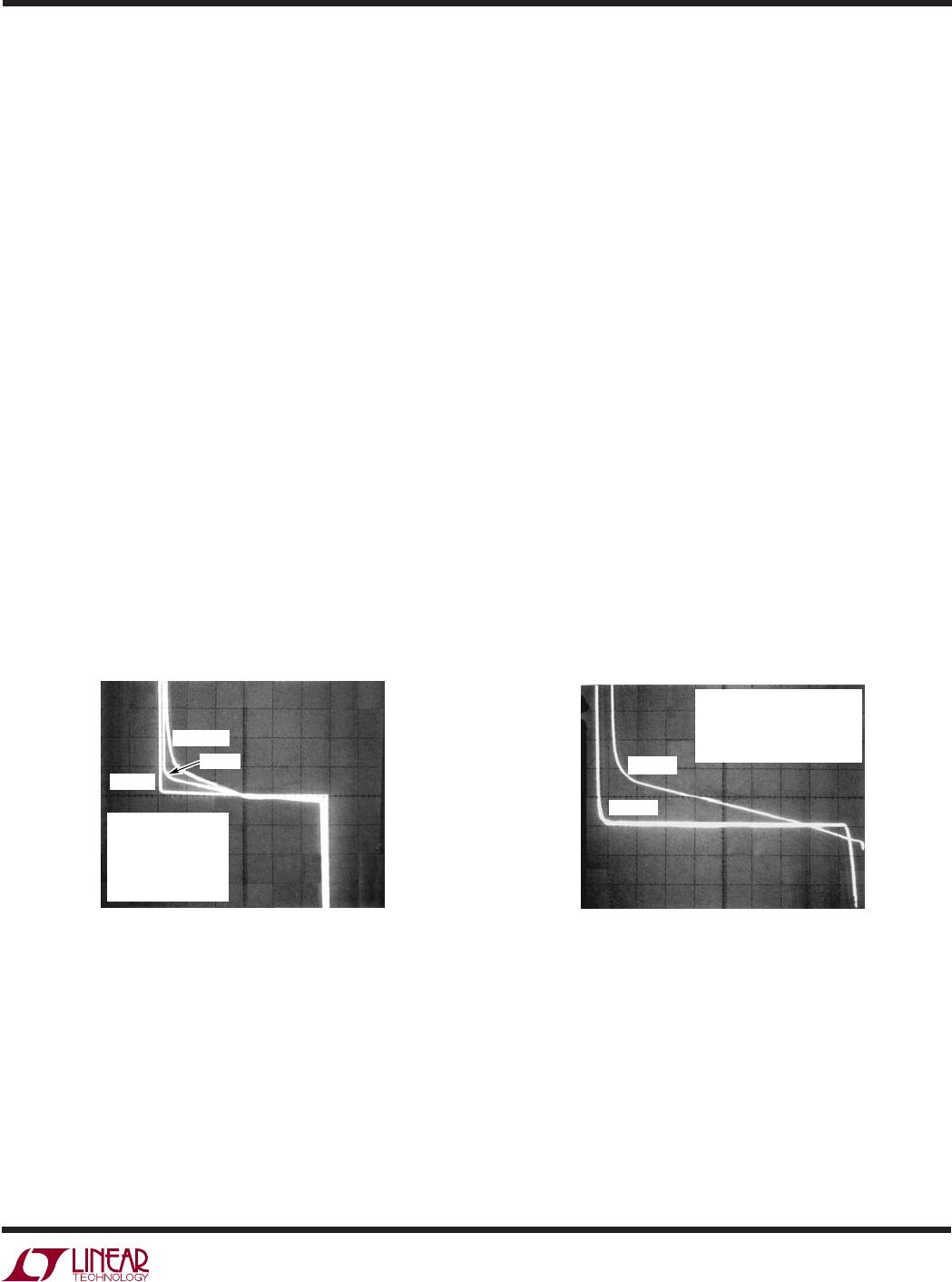
the gain. Figure 7 shows the change in input voltage for a
change in output voltage for different load resistors con-
nected between the supplies. The gain is much higher for
output voltages above ground (Q28 sources current) since
the change in base emitter voltage of Q28 is attenuated by
the gain in the PNP portion of the output stage. Therefore,
for positive output swings (output sourcing current) there
is hardly any change in input voltage for any load resistance.
Highest gain and best linearity are achieved when the output
is sourcing current, which is the case in single supply op-
eration when the load is ground referenced. Figure 8 shows
gains for both sinking and sourcing load currents for a
worst-case load of 600.
–15 –10 –5 0 5 10 15
OUTPUT VOLTAGE (V)
INPUT VOLTAGE
(50µV/DIV)
R
L
= 10k
R
L
= 600
R
L
= 1k
16789 F07
T
A
= 25°C
V
S
= ±15V
R
L
CONNECTED TO 0V
MEASURED ON
TEKTRONIX 577
CURVE TRACER
120354
OUTPUT VOLTAGE (V)
INPUT VOLTAGE
(10µV/DIV)
R
L
TO 5V
R
L
TO 0V
16789 F08
VOLTAGE GAIN SINGLE SUPPLY
V
S
= 5V
R
L
= 600
MEASURED ON TEKTRONIX 577
CURVE TRACER
Figure 7. Voltage Gain Split Supply Figure 8. Voltage Gain Single Supply
APPLICATIO S I FOR ATIO
WUUU
LT1678/LT1679
14
sn16789 16789fs
SI PLIFIED SCHE ATIC
WW
R8
200
R21
100
R13
100
R24
100
R9
200
Q1A
Q10
Q12
Q5
Q6
Q4 Q7
C10
81pF
R
C2
6k
R
C1
6k
Q11
Q3
IB
D4
D3
D1
D2
IC
ID
50µA
IA, IB = 0µA V
CM
> 1.5V ABOVE –V
S
200µA V
CM
< 1.5V ABOVE –V
S
IC = 200µA V
CM
< 0.7V BELOW +V
S
50µA V
CM
> 0.7V BELOW +V
S
ID = 100µA V
CM
< 0.7V BELOW +V
S
0µA V
CM
> 0.7V BELOW +V
S
IA
Q8 Q9
Q21
Q13
×2
Q2B
Q17
Q18
R15
1k
Q24
+
+IN
–IN
50µA
Q15
Q14 Q16
Q25
Q22
100µA
R14
1k
R16
1k
R25
1k
R30
2k
R26
100
R29
10
R23B
10k
R23A
10k
100µA
160µA
Q19
Q20
R20
2k
R2
50
R19
2k
200µA
Q38
Q23
C2
80pF
+
R32
1.5k
Q32
R34
2k
R54
100
R3
100
C3
40pF
C4
20pF
Q29
16789 SS
Q26
Q30
Q31
+
R1
500
C1
40pF
+
+
Q27
Q35
Q34
Q28
OUT
–V
S
+V
S
Q1B Q2A
LT1678/LT1679
15
sn16789 16789fs
U
PACKAGE DESCRIPTIO
.016 – .050
(0.406 – 1.270)
.010 – .020
(0.254 – 0.508)
× 45°
0°– 8° TYP
.008 – .010
(0.203 – 0.254)
SO8 0303
.053 – .069
(1.346 – 1.752)
.014 – .019
(0.355 – 0.483)
TYP
.004 – .010
(0.101 – 0.254)
.050
(1.270)
BSC
1
2
3
4
.150 – .157
(3.810 – 3.988)
NOTE 3
8
7
6
5
.189 – .197
(4.801 – 5.004)
NOTE 3
.228 – .244
(5.791 – 6.197)
.245
MIN
.160
±
.005
RECOMMENDED SOLDER PAD LAYOUT
.045
±
.005
.050 BSC
.030
±
.005
TYP
INCHES
(MILLIMETERS)
NOTE:
1. DIMENSIONS IN
2. DRAWING NOT TO SCALE
3. THESE DIMENSIONS DO NOT INCLUDE MOLD FLASH OR PROTRUSIONS.
MOLD FLASH OR PROTRUSIONS SHALL NOT EXCEED .006" (0.15mm)
S8 Package
8-Lead Plastic Small Outline (Narrow .150 Inch)
(Reference LTC DWG # 05-08-1610)
S Package
14-Lead Plastic Small Outline (Narrow .150 Inch)
(Reference LTC DWG # 05-08-1610)
1
N
2
3
4
.150 – .157
(3.810 – 3.988)
NOTE 3
14
13
.337 – .344
(8.560 – 8.738)
NOTE 3
.228 – .244
(5.791 – 6.197)
12
11
10
9
5
6
7
N/2
8
.016 – .050
(0.406 – 1.270)
.010 – .020
(0.254 – 0.508)
× 45°
0° – 8° TYP
.008 – .010
(0.203 – 0.254)
S14 0502
.053 – .069
(1.346 – 1.752)
.014 – .019
(0.355 – 0.483)
TYP
.004 – .010
(0.101 – 0.254)
.050
(1.270)
BSC
.245
MIN
N
1 2 3 N/2
.160 ±.005
RECOMMENDED SOLDER PAD LAYOUT
.045 ±.005
.050 BSC
.030 ±.005
TYP
INCHES
(MILLIMETERS)
NOTE:
1. DIMENSIONS IN
2. DRAWING NOT TO SCALE
3. THESE DIMENSIONS DO NOT INCLUDE MOLD FLASH OR PROTRUSIONS.
MOLD FLASH OR PROTRUSIONS SHALL NOT EXCEED .006" (0.15mm)
Information furnished by Linear Technology Corporation is believed to be accurate and reliable.
However, no responsibility is assumed for its use. Linear Technology Corporation makes no represen-
tation that the interconnection of its circuits as described herein will not infringe on existing patent rights.

LT1679CS#PBF

Mfr. #:
Manufacturer:
Analog Devices Inc.
Description:
Precision Amplifiers Quad Low Noise R-to-R Pre OA
Lifecycle:
New from this manufacturer.
Delivery:
DHL FedEx Ups TNT EMS
Payment:
T/T Paypal Visa MoneyGram Western Union