DS1238
4 of 14
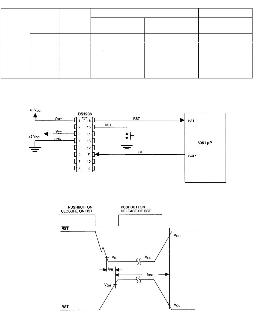
Table 1. The WDS pin will remain low until one of three operations occurs. The first is to strobe the ST
pin with a falling edge, which will both set the WDS as well as the watchdog timer count. The second is
to leave the ST pin open, which disables the watchdog. Lastly, the WDS pin is active low whenever V
CC
falls below V
CCTP
and activates the RVT signal. The ST input can be derived from microprocessor
address, data, or control signals, as well as microcontroller port pins. Under normal operating conditions,
these signals would routinely reset the watchdog timer prior to time out. The watchdog is disabled by
leaving the
ST input open, or as soon as V
CC
falls to V
CCTP
.
NON-MASKABLE INTERRUPT
The DS1238 generates a non-maskable interrupt ( NMI ) for early warning of a power failure to the
microprocessor. A precision comparator monitors the voltage level at the IN pin relative to an on-chip
reference generated by an internal band gap. The IN pin is a high impedance input allowing for a user-
defined sense point. An external resistor voltage divider network (Figure 5) is used to interface with high
voltage signals. This sense point may be derived from the regulated 5-volt supply, or from a higher DC
voltage level closer to the main system power input. Since the IN trip point V
TP
is 1.27 volts, the proper
values for R1 and R2 can be determined by the equation as shown in Figure 5. Proper operation of the
DS1238 requires that the voltage at the IN pin be limited to V
IH
. Therefore, the maximum allowable
voltage at the supply being monitored (V
MAX
) can also be derived as shown in Figure 5. A simple
approach to solving this equation is to select a value for R2 of high enough value to keep power
consumption low and solve for R1. The flexibility of the IN input pin allows for detection of power loss
at the earliest point in a power supply system, maximizing the amount of time for microprocessor
shutdown between NMI and RST or RST .
When the supply being monitored decays to the voltage sense point, the DS1238 will force the NMI
output to an active state. Noise is removed from the NMI power-fail detection circuitry using built-in
time domain hysteresis. That is, the monitored supply is sampled periodically at a rate determined by an
internal ring oscillator running at approximately 30kHz (33 µs/cycle). Three consecutive samplings of
out-of-tolerance supply (below V
SENSE
) must occur at the IN pin to active NMI . Therefore, the supply
must be below the voltage sense point for approximately 100 µs or the comparator will reset. In this way,
power supply noise is removed from the monitoring function preventing false trips. During a power-up,
any IN pin levels below V
TP
detected by the comparator are disabled from reaching the NMI I pin until
V
CC
rises to V
CCTP
. As a result, any potential active NMI will not be initiated until V
CC
reaches V
CCTP
.
Removal of an active low level on the
NMI pin is controlled by the subsequent rise of the IN pin above
V
TP
. The initiation and removal of the NMI signal during power up depends on the relative voltage
relationship between V
CC
and the IN pin voltage. Note that a fast-slewing power supply may cause the
NMI to be virtually nonexistent on power up. This is of no consequence, however, since an RST will be
active. The NMI voltage will follow V
CC
down until V
CC
decays to V
BAT
. Once V
CC
decays to V BAT , the
NMI pin will enter a tri-state mode.
ST INPUT TIMING Figure 2