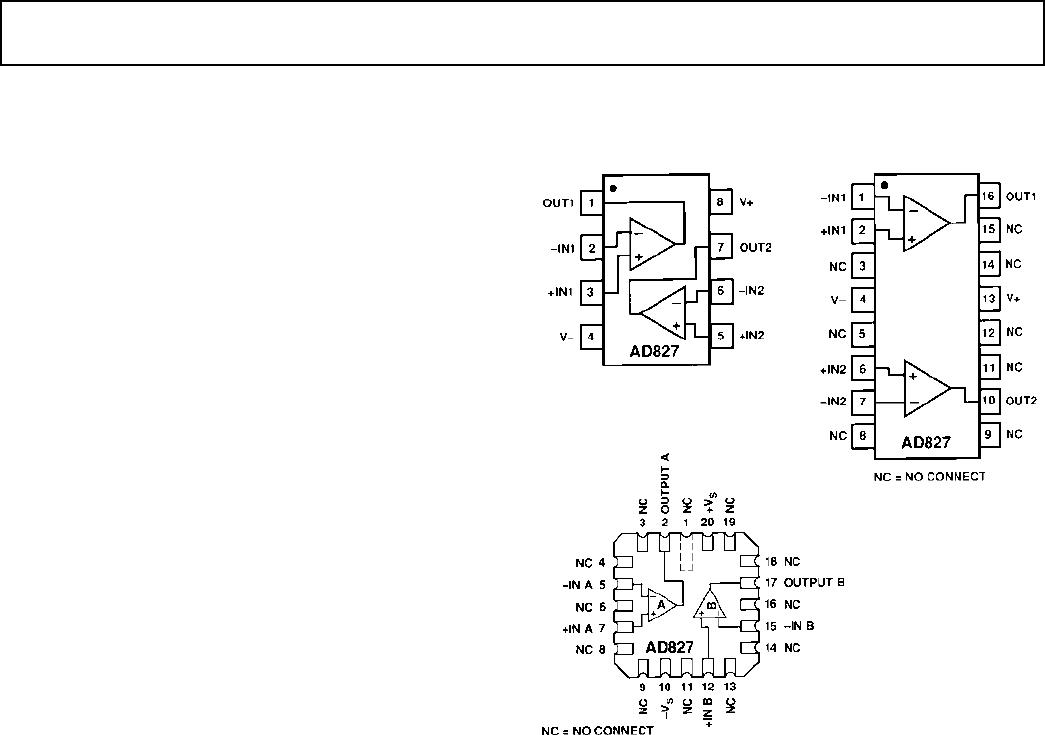
CONNECTION DIAGRAMS
a
High Speed, Low Power
Dual Op Amp
AD827
FEATURES
High Speed
50 MHz Unity Gain Stable Operation
300 V/ms Slew Rate
120 ns Settling Time
Drives Unlimited Capacitive Loads
Excellent Video Performance
0.04% Differential Gain @ 4.4 MHz
0.198 Differential Phase @ 4.4 MHz
Good DC Performance
2 mV max Input Offset Voltage
15 mV/8C Input Offset Voltage Drift
Available in Tape and Reel in Accordance with
EIA-481A Standard
Low Power
Only 10 mA Total Supply Current for Both Amplifiers
5 V to 15 V Supplies
PRODUCT DESCRIPTION
The AD827 is a dual version of Analog Devices’ industry-
standard AD847 op amp. Like the AD847, it provides high
speed, low power performance at low cost. The AD827 achieves
a 300 V/µs slew rate and 50 MHz unity-gain bandwidth while
consuming only 100 mW when operating from ±5 volt power
supplies. Performance is specified for operation using ±5 V to
±15 V power supplies.
The AD827 offers an open-loop gain of 3,500 V/V into 500
loads. It also features a low input voltage noise of 15 nV/Hz,
and a low input offset voltage of 2 mV maximum. Common-
mode rejection ratio is a minimum of 80 dB. Power supply
rejection ratio is maintained at better than 20 dB with input
frequencies as high as 1 MHz, thus minimizing noise
feedthrough from switching power supplies.
The AD827 is also ideal for use in demanding video applica-
tions, driving coaxial cables with less than 0.04% differential
gain and 0.19° differential phase errors for 643 mV p-p into a
75 reverse terminated cable.
The AD827 is also useful in multichannel, high speed data
conversion systems where its fast (120 ns to 0.1%) settling time
is of importance. In such applications, the AD827 serves as an
input buffer for 8-bit to 10-bit A/D converters and as an output
amplifier for high speed D/A converters.
APPLICATION HIGHLIGHTS
1. Performance is fully specified for operation using ±5 V to
±15 V supplies.
2. A 0.04% differential gain and 0.19° differential phase error at
the 4.4 MHz color subcarrier frequency, together with its low
cost, make it ideal for many video applications.
3. The AD827 can drive unlimited capacitive loads, while its
30 mA output current allows 50 and 75 reverse-
terminated loads to be driven.
4. The AD827’s 50 MHz unity-gain bandwidth makes it an
ideal candidate for multistage active filters.
5. The AD827 is available in 8-lead plastic mini-DIP and cerdip,
20-lead LCC, and 16-lead SOIC packages. Chips and
MIL-STD-883B processing are also available.
8-Lead Plastic (N) and Cerdip
(Q) Packages
16-Lead Small Outline
(R) Package
20-Lead LCC (E) Package
REV. C
Information furnished by Analog Devices is believed to be accurate and
reliable. However, no responsibility is assumed by Analog Devices for its
use, nor for any infringements of patents or other rights of third parties that
may result from its use. No license is granted by implication or otherwise
under any patent or patent rights of Analog Devices.
One Technology Way, P.O. Box 9106, Norwood, MA 02062-9106, U.S.A.
Tel: 781/329-4700 www.analog.com
Fax: 781/326-8703 © Analog Devices, Inc., 2002
AD827* PRODUCT PAGE QUICK LINKS
Last Content Update: 02/23/2017
COMPARABLE PARTS
View a parametric search of comparable parts.
DOCUMENTATION
Application Notes
AN-402: Replacing Output Clamping Op Amps with Input
Clamping Amps
AN-417: Fast Rail-to-Rail Operational Amplifiers Ease
Design Constraints in Low Voltage High Speed Systems
AN-581: Biasing and Decoupling Op Amps in Single
Supply Applications
Data Sheet
AD827: High Speed, Low Power Dual Op Amp Data Sheet
AD827: Military Data Sheet
TOOLS AND SIMULATIONS
Analog Filter Wizard
Analog Photodiode Wizard
Power Dissipation vs Die Temp
VRMS/dBm/dBu/dBV calculators
AD827 SPICE Macro Model
REFERENCE MATERIALS
Product Selection Guide
High Speed Amplifiers Selection Table
Tutorials
MT-032: Ideal Voltage Feedback (VFB) Op Amp
MT-047: Op Amp Noise
MT-048: Op Amp Noise Relationships: 1/f Noise, RMS
Noise, and Equivalent Noise Bandwidth
MT-049: Op Amp Total Output Noise Calculations for
Single-Pole System
MT-050: Op Amp Total Output Noise Calculations for
Second-Order System
MT-052: Op Amp Noise Figure: Don't Be Misled
MT-053: Op Amp Distortion: HD, THD, THD + N, IMD,
SFDR, MTPR
MT-056: High Speed Voltage Feedback Op Amps
MT-058: Effects of Feedback Capacitance on VFB and CFB
Op Amps
MT-060: Choosing Between Voltage Feedback and
Current Feedback Op Amps
DESIGN RESOURCES
AD827 Material Declaration
PCN-PDN Information
Quality And Reliability
Symbols and Footprints
DISCUSSIONS
View all AD827 EngineerZone Discussions.
SAMPLE AND BUY
Visit the product page to see pricing options.
TECHNICAL SUPPORT
Submit a technical question or find your regional support
number.
DOCUMENT FEEDBACK
Submit feedback for this data sheet.
This page is dynamically generated by Analog Devices, Inc., and inserted into this data sheet. A dynamic change to the content on this page will not
trigger a change to either the revision number or the content of the product data sheet. This dynamic page may be frequently modified.
REV. C
–2–
AD827–SPECIFICATIONS
(@ T
A
= +25C, unless otherwise noted.)
AD827J AD827A/S
Model Conditions V
S
Min Typ Max Min Typ Max Unit
DC PERFORMANCE
Input Offset Voltage
1
±5 V 0.5 2 0.3 2 mV
T
MIN
to T
MAX
3.5 4 mV
±15 V 4 4 mV
T
MIN
to T
MAX
66mV
Offset Voltage Drift ±5 V to ±15 V 15 15 µV/°C
Input Bias Current ±5 V to ±15 V 3.3 7 3.3 7 µA
T
MIN
to T
MAX
8.2 9.5 µA
Input Offset Current ±5 V to ±15 V 50 300 50 300 nA
T
MIN
to T
MAX
400 400 nA
Offset Current Drift ±5 V to ±15 V 0.5 0.5 nA/°C
Common-Mode Rejection Ratio V
CM
= ±2.5 V ±5 V 78 95 8095 dB
V
CM
= ±12 V ±15 V 78 95 8095 dB
T
MIN
to T
MAX
±5 V to ±15 V 75 75dB
Power Supply Rejection Ratio ±5 V to ±15 V 75 86 7586 dB
T
MIN
to T
MAX
72 72 dB
Open-Loop Gain
V
O
= ±2.5 V ±5 V
R
LOAD
= 500 2 3.5 2 3.5 V/mV
T
MIN
to T
MAX
11V/mV
R
LOAD
= 150 1.6 1.6 V/mV
V
OUT
= ±10 V ±15 V
R
LOAD
= 1 k 3 5.5 3 5.5 V/mV
T
MIN
to T
MAX
1.5 1.5 V/mV
MATCHING CHARACTERISTICS
Input Offset Voltage ±5 V 0.4 0.2 mV
Crosstalk f = 5 MHz ±5 V 85 85 dB
DYNAMIC PERFORMANCE
Unity-Gain Bandwidth ±5 V 35 35 MHz
±15 V 50 50 MHz
Full Power Bandwidth
2
V
O
= 5 V p-p,
R
LOAD
= 500 Ω±5 V 12.7 12.7 MHz
V
O
= 20 V p-p,
R
LOAD
= 1 kΩ±15 V 4.7 4.7 MHz
Slew Rate
3
R
LOAD
= 500 Ω±5 V 200 200 V/µs
R
LOAD
= 1 kΩ±15 V 300 300 V/µs
Settling Time to 0.1% A
V
= –1
–2.5 V to +2.5 V ±5 V 65 65 ns
–5 V to +5 V ±15 V 120 120 ns
Phase Margin C
LOAD
= 10 pF ± 15 V
R
LOAD
= 1 k 50 50 Degrees
Differential Gain Error f = 4.4 MHz ±15 V 0.04 0.04 %
Differential Phase Error f = 4.4 MHz ±15 V 0.19 0.19 Degrees
Input Voltage Noise f = 10 kHz ±15 V 15 15 nV/Hz
Input Current Noise f = 10 kHz ± 15 V 1.5 1.5 pA/Hz
Input Common-Mode
Voltage Range ±5 V +4.3 +4.3 V
–3.4 –3.4 V
±15 V +14.3 +14.3 V
–13.4 –13.4 V
Output Voltage Swing R
LOAD
= 500 Ω±5 V 3.0 3.6 3.0 3.6 ±V
R
LOAD
= 150 Ω±5 V 2.5 3.0 2.5 3.0 ±V
R
LOAD
= 1 kΩ±15 V 12 13.3 12 13.3 ±V
R
LOAD
= 500 Ω±15 V 10 12.2 10 12.2 ±V
Short-Circuit Current Limit ±5 V to ±15 V 32 32 mA
INPUT CHARACTERISTICS
Input Resistance 300 300 k
Input Capacitance 1.5 1.5 pF

AD827JRZ-16

Mfr. #:
Manufacturer:
Analog Devices Inc.
Description:
Precision Amplifiers DUAL HIGH Speed IC
Lifecycle:
New from this manufacturer.
Delivery:
DHL FedEx Ups TNT EMS
Payment:
T/T Paypal Visa MoneyGram Western Union