AD827J AD827A/S
Model Conditions V
S
Min Typ Max Min Typ Max Unit
OUTPUT RESISTANCE Open Loop 15 15 Ω
POWER SUPPLY
Operating Range ±4.5 ± 18 ±4.5 ± 18 V
Quiescent Current ±5 V 10 13 1013 mA
T
MIN
to T
MAX
16 16.5/17.5 mA
±15 V 10.5 13.5 10.5 13.5 mA
T
MIN
to T
MAX
16.5 17/18 mA
TRANSISTOR COUNT 92 92
NOTES
1
Offset voltage for the AD827 is guaranteed after power is applied and the device is fully warmed up. All other specifications are measured using high speed test equipment,
approximately 1 second after power is applied.
2
Full Power Bandwidth = Slew Rate/2 π V
PEAK
.
3
Gain = +1, rising edge.
All min and max specifications are guaranteed.
Specifications subject to change without notice.
ABSOLUTE MAXIMUM RATINGS
1
Supply Voltage . . . . . . . . . . . . . . . . . . . . . . . . . . . . . . . . ±18 V
Internal Power Dissipation
2
Plastic (N) Package (Derate at 10 mW/°C) . . . . . . . . 1.5 W
Cerdip (Q) Package (Derate at 8.7 mW/°C) . . . . . . . 1.3 W
Small Outline (R) Package (Derate at 10 mW/°C) . . . 1.5 W
LCC (E) Package (Derate at 6.7 mW/°C) . . . . . . . . . 1.0 W
Input Common-Mode Voltage . . . . . . . . . . . . . . . . . . . . . ±V
S
Differential Input Voltage . . . . . . . . . . . . . . . . . . . . . . . . . 6 V
Output Short Circuit Duration
3
. . . . . . . . . . . . . . . . Indefinite
Storage Temperature Range (N, R) . . . . . . . –65°C to +125°C
Storage Temperature Range (Q) . . . . . . . . . –65°C to +150°C
Operating Temperature Range
AD827J . . . . . . . . . . . . . . . . . . . . . . . . . . . . . . 0°C to 70°C
AD827A . . . . . . . . . . . . . . . . . . . . . . . . . . . –40°C to +85°C
AD827S . . . . . . . . . . . . . . . . . . . . . . . . . . –55°C to +125°C
Lead Temperature Range
(Soldering to 60 sec) . . . . . . . . . . . . . . . . . . . . . . . . . 300°C
NOTES
1
Stresses above those listed under Absolute Maximum Ratings may cause perma-
nent damage to the device. This is a stress rating only, and functional operation of
the device at these or any other conditions above those indicated in the operational
section of this specification is not implied. Exposure to absolute maximum ratings
for extended periods may affect device reliability.
2
Maximum internal power dissipation is specified so that T
J
does not exceed 175°C
at an ambient temperature of 25°C.
Thermal Characteristics:
MiniDIP: θ
JA
= 100°C/W; θ
JC
= 33°C/ W
Cerdip: θ
JA
= 110°C/W; θ
JC
= 30°C/W
16-Lead Small Outline Package: θ
JA
= 100°C/W
20-Lead LCC: θ
JA
= 150°C/W;
θ
JC
= 35°C/W
3
Indefinite short circuit duration is only permissible as long as the absolute
maximum power rating is not exceeded.
ORDERING GUIDE
Temperature Package Package
Model Range Description Option
AD827JN 0°C to +70°C8-Lead Plastic DIP N-8
AD827JR 0°C to +70°C 16-Lead Plastic SO R-16
AD827AQ –40°C to +85°C8-Lead Cerdip Q-8
AD827SQ –55°C to +125°C8-Lead Cerdip Q-8
AD827SQ/883B –55°C to +125°C8-Lead Cerdip Q-8
5962-9211701MPA –55°C to +125°C8-Lead Cerdip Q-8
AD827SE/883B –55°C to +125°C 20-Lead LCC E-20A
5962-9211701M2A –55°C to +125°C 20-Lead LCC E-20A
AD827JR-REEL 0°C to +70°CTape & Reel
AD827JChips 0°C to +70°CDie
AD827SChips –55°C to +125°CDie
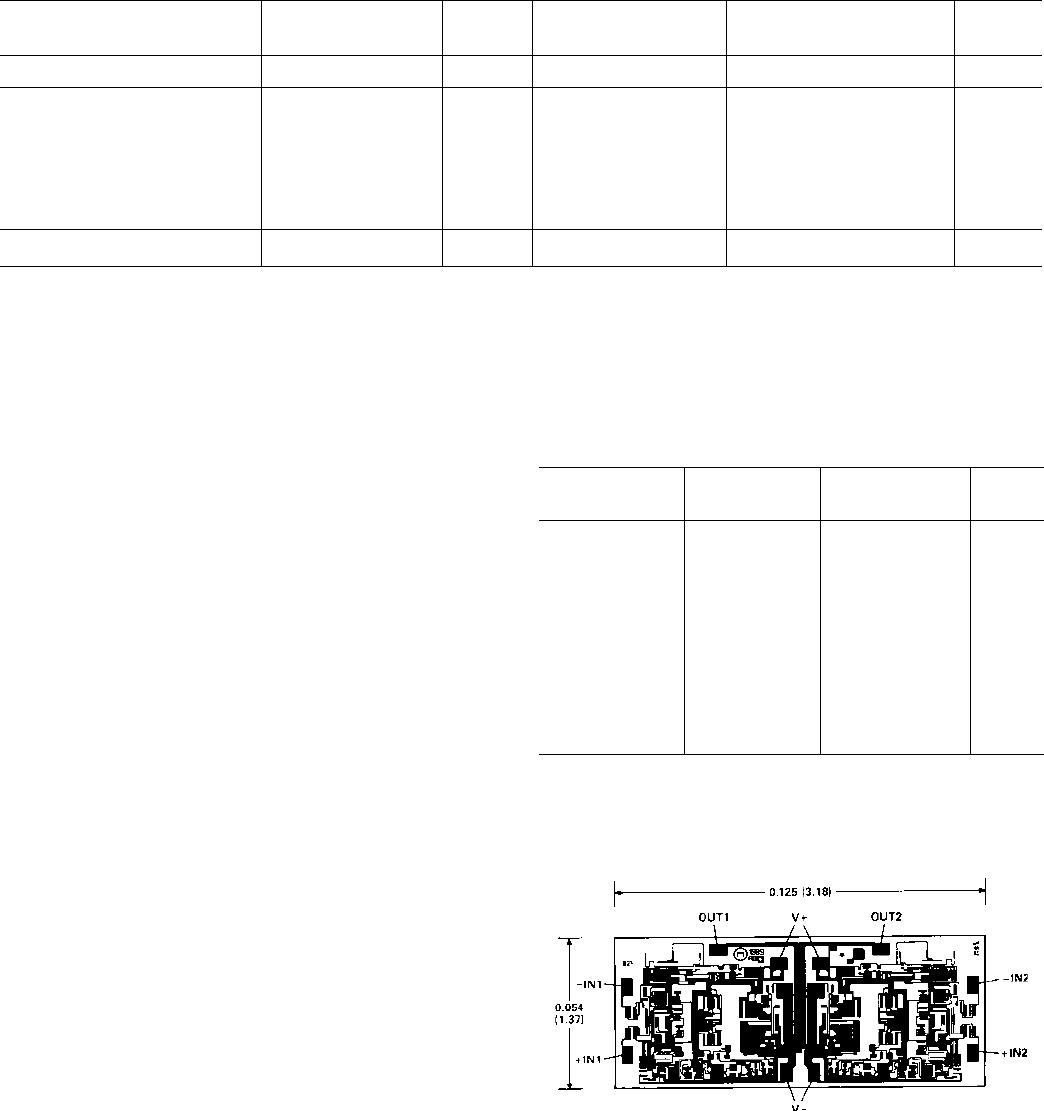
METALLIZATION PHOTOGRAPH
Contact factory for latest dimensions.
Dimensions shown in inches and (mm).
Substrate is connected to V+.
AD827
REV. C
–3–