AD827
REV. C
–6–
Figure 19. Crosstalk vs. Frequency
Figure 20. Crosstalk Test Circuit
INPUT PROTECTION PRECAUTIONS
An input resistor (resistor R
IN
of Figure 21a) is recommended in
circuits where the input common-mode voltage to the AD827
may exceed (on a transient basis) the positive supply voltage.
This resistor provides protection for the input transistors by
limiting the maximum current that can be forced into their bases.
Figure 21c. Follower Small
Signal Pulse Response
Figure 22c. Inverter Small
Signal Pulse Response
Figure 21b. Follower Large
Signal Pulse Response
Figure 22b. Inverter Large
Signal Pulse Response
Figure 21a. Follower Connection
Figure 22a. Inverter Connection
For high performance circuits, it is recommended that a second
resistor (R
B
in Figures 21a and 22a) be used to reduce bias-
current errors by matching the impedance at each input. This
resistor reduces the error caused by offset voltages by more than
an order of magnitude.
AD827
REV. C
–7–
VIDEO LINE DRIVER
The AD827 functions very well as a low cost, high speed line
driver for either terminated or unterminated cables. Figure 23
shows the AD827 driving a doubly terminated cable in a
follower configuration.
0.1 µF
0.1 µF
50
AD827
1/2
R
BT
C
C
+V
S
V
IN
V
OU
T
–V
S
R
T
500
50
50
500
Figure 23. A Video Line Driver
The termination resistor, R
T
, (when equal to the cable’s
characteristic impedance) minimizes reflections from the far end
of the cable. While operating from ±5 V supplies, the AD827
maintains a typical slew rate of 200 V/µs, which means it can
drive a ±1 V, 30 MHz signal into a terminated cable.
Table I. Video Line Driver Performance Summary
Over-
V
IN
* V
SUPPLY
C
C
–3 dB B
W
shoot
0 dB or ±500 mV Step ±15 20 pF 23 MHz 4%
0 dB or ±500 mV Step ±15 15 pF 21 MHz 0%
0 dB or ±500 mV Step ±15 0 pF 13 MHz 0%
0 dB or ±500 mV Step ±5 20 pF 18 MHz 2%
0 dB or ±500 mV Step ±5 15 pF 16 MHz 0%
0 dB or ±500 mV Step ±50 pF11 MHz 0%
*–3 dB bandwidth numbers are for the 0 dBm signal input. Overshoot numbers
are the percent overshoot of the 1 V step input.
A back-termination resistor (R
BT
, also equal to the characteristic
impedance of the cable) may be placed between the AD827
output and the cable input, in order to damp any reflected
signals caused by a mismatch between R
T
and the cable’s
characteristic impedance. This will result in a flatter frequency
response, although this requires that the op amp supply ±2 V to
the output in order to achieve a ±1 V swing at resistor R
T
.
A HIGH SPEED THREE OP AMP INSTRUMENTATION
AMPLIFIER CIRCUIT
The instrumentation amplifier circuit shown in Figure 24 can
provide a range of gains. Table II details performance.
+
+
+
1
3
2
2
3
6
7
6
5
AD847
AD827
AD827
0.1µF
1k
2k
2k
1k
2k
0.1µF
0.1µF
2k
R
L
2 – 8pF
0.1µF
R
G
4
7
2k
8
4
TRIM FOR BEST
SETTLING TIME
1/2
1/2
3pF
CIRCUIT GAIN =
+ 1
G
R
2000
TRIM FOR
OPTIMUM
BANDWIDTH
7 – 15 pF
NOTE: PINOUT SHOWN IS FOR MINIDIP PACKAGE
–V
IN
+V
S
–V
S
+V
IN
+V
S
–V
S
V
OUT
Figure 24. A High Bandwidth Three Op Amp
Instrumentation Amplifier
Table II. Performance Specifications for the
Three Op Amp Instrumentation Amplifier
Small Signal
Bandwidth
Gain R
G
@ 1 V p-p Output
1 Open 16.1 MHz
22 k 14.7 MHz
10 226 4.9 MHz
100 20 660 kHz
AD827
REV. C
–8–
multipliers connected in series. They could also be placed in
parallel with an increase in bandwidth and a reduction in gain.
The gain of the circuit is controlled by V
X
, which can range
from 0 to 3 V dc. Measurements show that this circuit easily
supplies 2 V p-p into a 100 load while operating from ±5 V
supplies. The overall bandwidth of the circuit is approximately
7 MHz with 0.5 dB of peaking.
Each half of the AD827 serves as an I/V converter and converts
the output current of one of the two multipliers in the AD539
into an output voltage. Each of the AD539’s two multipliers
contains two internal 6 k feedback resistors; one is connected
between the CH1 output and Z1, the other between the CH1
output and W1. Likewise, in the CH2 multiplier, one of the
feedback resistors is connected between CH2 and Z2 and the
other is connected between CH2 and Z2. In Figure 25, Z1 and
W1 are tied together, as are Z2 and W2, providing a 3 k
feedback resistor for the op amp. The 2 pF capacitors connected
between the AD539’s W1 and CH1 and W2 and CH2 pins are
in parallel with the feedback resistors and thus reduce peaking
in the VCA’s frequency response. Increasing the values of C3
and C4 can further reduce the peaking at the expense of
reduced bandwidth. The 1.25 mA full-scale output current of
the AD539 and the 3 k feedback resistor set the full-scale
output voltage of each multiplier at 3.25 V p-p.
Current limiting in the AD827 (typically 30 mA) limits the out-
put voltage in this application to about 3 V p-p across a 100
load. Driving a 50 reverse-terminated load divides this value
by two, limiting the maximum signal delivered to a 50 load to
about 1.5 V p-p, which suffices for video signal levels. The
dynamic range of this circuit is approximately 55 dB and is
primarily limited by feedthrough at low input levels and by the
maximum output voltage at high levels.
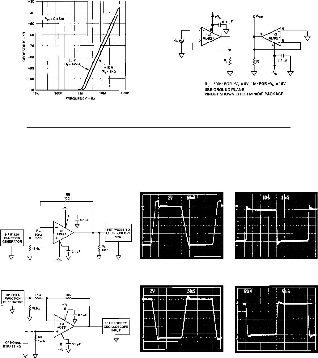
Guidelines for Grounding and Bypassing
When designing practical high frequency circuits using the AD827,
some special precautions are in order. Both short interconnection
leads and a large ground plane are needed whenever possible to
provide low resistance, low inductance circuit paths. One should
remember to minimize the effects of capacitive coupling
between circuits. Furthermore, IC sockets should be avoided.
Feedback resistors should be of a low enough value that the
time constant formed with stray circuit capacitances at the
amplifier summing junction will not limit circuit performance.
As a rule of thumb, use feedback resistor values that are less
than 5 k. If a larger resistor value is necessary, a small (<10 pF)
feedback capacitor in parallel with the feedback resistor may be
used. The use of 0.1 µF ceramic disc capacitors is recommended
for bypassing the op amp’s power supply leads.
A TWO-CHIP VOLTAGE-CONTROLLED AMPLIFIER
(VCA) WITH EXPONENTIAL RESPONSE
Voltage-controlled amplifiers are often used as building blocks
in automatic gain control systems. Figure 25 shows a two-chip
VCA built using the AD827 and the AD539, a dual, current-
output multiplier. As configured, the circuit has its two
Figure 25. A Wide Range Voltage-Controlled
Amplifier Circuit

AD827JRZ-16

Mfr. #:
Manufacturer:
Analog Devices Inc.
Description:
Precision Amplifiers DUAL HIGH Speed IC
Lifecycle:
New from this manufacturer.
Delivery:
DHL FedEx Ups TNT EMS
Payment:
T/T Paypal Visa MoneyGram Western Union