AD797 Data Sheet
Rev. K | Page 12 of 19
NOISE AND SOURCE IMPEDANCE CONSIDERATIONS
The AD797 ultralow voltage noise of 0.9 nV/√Hz is achieved
with special input transistors running at nearly 1 mA of collector
current. Therefore, it is important to consider the total input-
referred noise (e
N
total), which includes contributions from voltage
noise (e
N
), current noise (i
N
), and resistor noise (√4 kTR
S
).
2/12
2
])(4[
S
N
S
NN
RikTRetotale (1)
where R
S
is the total input source resistance.
This equation is plotted for the AD797 in Figure 34. Because
optimum dc performance is obtained with matched source
resistances, this case is considered even though it is clear from
Equation 1 that eliminating the balancing source resistance
lowers the total noise by reducing the total R
S
by a factor of 2.
At very low source resistance (R
S
< 50 Ω), the voltage noise of the
amplifier dominates. As source resistance increases, the Johnson
noise of R
S
dominates until a higher resistance of R
S
> 2 kΩ is
achieved; the current noise component is larger than the
resistor noise.
00846-033
100
1
0.1
10
10 100 1000 10000
SOURCE RESISTANCE ()
NOISE (nV/
Hz)
TOTAL NOISE
RESISTOR
NOISE
ONLY
Figure 34. Noise vs. Source Resistance
The AD797 is the optimum choice for low noise performance if
the source resistance is kept <1 kΩ. At higher values of source
resistance, optimum performance with respect to only noise is
obtained with other amplifiers from Analog Devices (Table 5).
For up to date information, see AN-940.
Table 5. Recommended Amplifiers for Different Source
Impedances
R
S
(kΩ) Recommended Amplifier
0 to <1
AD8597/AD8599, AD797, ADA4004-1/
ADA4004-2/ADA4004-4, AD8671/AD8672/
AD8674
1 to <10
AD8675/AD8676, ADA4075-2, ADA4004-1/
ADA4004-2/ADA4004-4, OP1177, OP27/OP37,
OP184
10 to <100 AD8677, OP1177, OP2177, OP4177, OP471
>100
AD8610/AD8620, AD8605/AD8606/AD8608,
ADA4627-1, OP97, AD548, AD549, AD745
LOW FREQUENCY NOISE
Analog Devices specifies low frequency noise as a peak-to-peak
quantity in a 0.1 Hz to 10 Hz bandwidth. Several techniques can
be used to make this measurement. The usual technique involves
amplifying, filtering, and measuring the amplifier noise for a
predetermined test time. The noise bandwidth of the filter is
corrected for, and the test time is carefully controlled because
the measurement time acts as an additional low frequency roll-off.
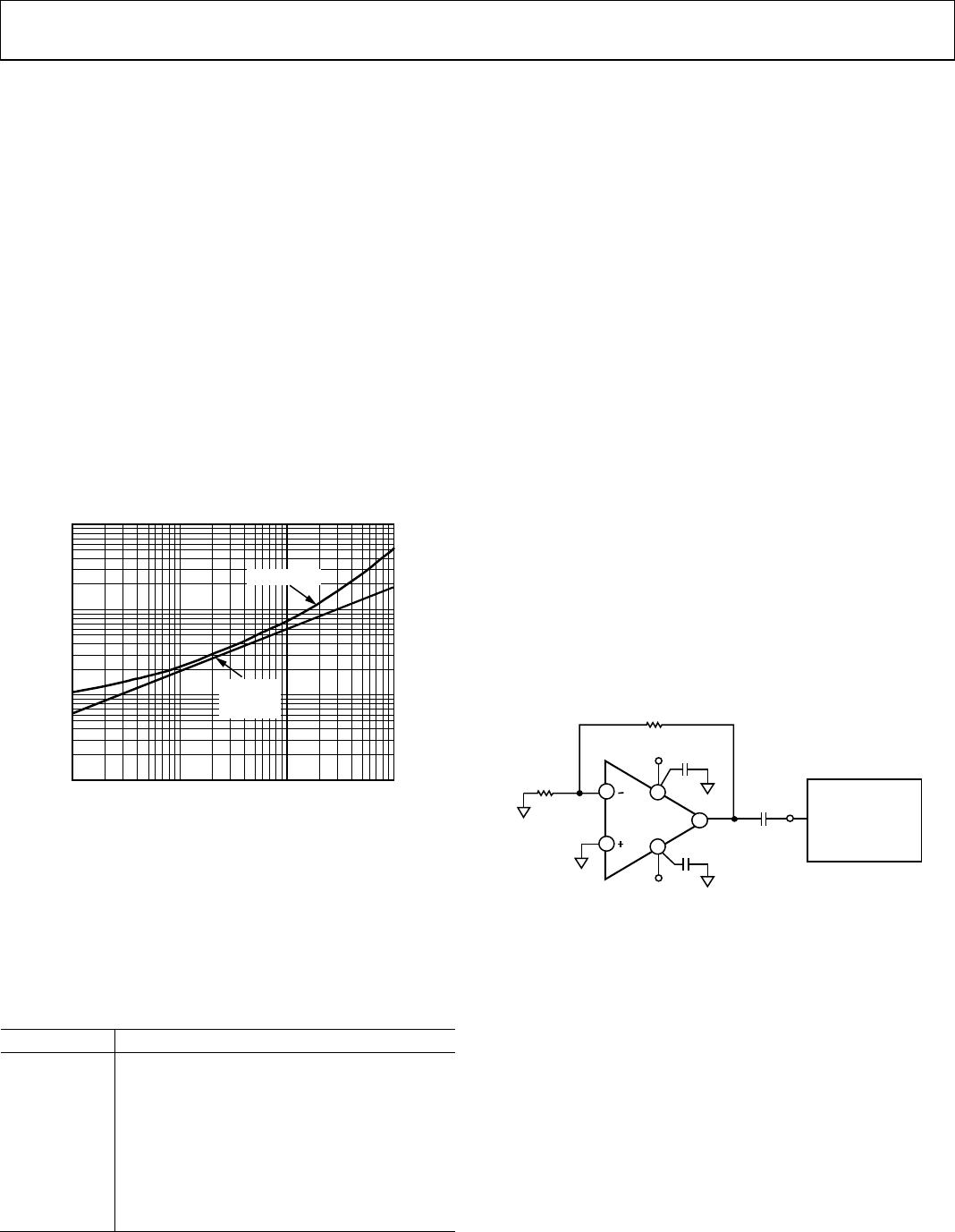
The plot in Figure 6 uses a slightly different technique: an FFT-
based instrument (Figure 35) is used to generate a 10 Hz brickwall
filter. A low frequency pole at 0.1 Hz is generated with an
external ac coupling capacitor, which is also the instrument being
dc coupled.
Several precautions are necessary to attain optimum low
frequency noise performance:
Care must be used to account for the effects of R
S
. Even
a 10 Ω resistor has 0.4 nV/√Hz of noise (an error of 9%
when root sum squared with 0.9 nV/√Hz).
The test setup must be fully warmed up to prevent e
OS
drift
from erroneously contributing to input noise.
Circuitry must be shielded from air currents. Heat flow out
of the package through its leads creates the opportunity for
a thermoelectric potential at every junction of different metals.
Selective heating and cooling of these by random air currents
appears as 1/f noise and obscures the true device noise.
The results must be interpreted using valid statistical
techniques.
7
4
6
2
3
HP 3465
DYNAMIC SIGNAL
ANALYZER
(10Hz)
1
100k
*
*
V
OUT
+V
S
–V
S
1.5µF
AD797
00846-034
*USE THE POWER SUPPLY BYPASSING SHOWN IN FIGURE 36.
Figure 35. Test Setup for Measuring 0.1 Hz to 10 Hz Noise
WIDEBAND NOISE
Due to its single-stage design, the noise of the AD797 is flat
over frequencies from less than 10 Hz to beyond 1 MHz. This
is not true of most dc precision amplifiers, where second-stage
noise contributes to input-referred noise beyond the audio
frequency range. The AD797 offers new levels of performance in
wideband imaging applications. In sampled data systems, where
aliasing of out-of-band noise into the signal band is a problem,
the AD797 outperforms all previously available IC op amps.
Data Sheet AD797
Rev. K | Page 13 of 19
BYPASSING CONSIDERATIONS
Taking full advantage of the very wide bandwidth and dynamic
range capabilities of the AD797 requires some precautions.
First, multiple bypassing is recommended in any precision
application. A 1.0 μF to 4.7 μF tantalum in parallel with 0.1 μF
ceramic bypass capacitors are sufficient in most applications.
When driving heavy loads, a larger demand is placed on the
supply bypassing. In this case, selective use of larger values of
tantalum capacitors and damping of their lead inductance with
small-value (1.1 Ω to 4.7 Ω) carbon resistors can achieve an
improvement. Figure 36 summarizes power supply bypassing
recommendations.
USE SHORT
LEAD LENGTHS
(<5mm)
KELVIN RETURN
LOAD
CURRENT
OR
0
.1µ
F
S
S
4.7µF
00846-035
USE SHORT
LEAD LENGTHS
(<5mm)
KELVIN RETURN
LOAD
CURRENT
0.1µF 4.7µF TO 22.0µF
1.1 TO 4.7
Figure 36. Recommended Power Supply Bypassing
THE NONINVERTING CONFIGURATION
Ultralow noise requires very low values of the internal parasitic
resistance (r
BB
) for the input transistors (≈6 Ω). This implies
very little damping of input and output reactive interactions.
With the AD797, additional input series damping is required
for stability with direct output to input feedback. A 100 Ω
resistor (R1) in the inverting input (see Figure 37) is sufficient;
the 100 Ω balancing resistor (R2) is recommended but is not
required for stability. The noise penalty is minimal (e
N
total ≈
2.1 nV/√Hz), which is usually insignificant.
7
4
3
R2
100
R1
100
*
*
V
O
U
T
V
I
N
+V
S
–V
S
AD797
00846-036
R
L
600
6
2
*
USE THE POWER SUPPLY BYPASSING SHOWN IN FIGURE 35.
Figure 37. Voltage Follower Connection
Best response flatness is obtained with the addition of a small
capacitor (C
L
< 33 pF) in parallel with the 100 Ω resistor
(Figure 38). The input source resistance and capacitance also
affect the response slightly, and experimentation may be
necessary for best results.
7
*
*USE THE POWER SUPPLY BYPASSING SHOWN IN FIGURE 35.
*
V
O
U
T
V
I
N
+V
S
–V
S
AD797
00846-037
C
L
6
2
R
S
C
S
3
4
600
100
Figure 38. Alternative Voltage Follower Connection
Low noise preamplification is usually performed in the non-
inverting mode (see Figure 39). For lowest noise, the equivalent
resistance of the feedback network should be as low as possible.
The 30 mA minimum drive current of the AD797 makes it easier
to achieve this. The feedback resistors can be made as low as
possible, with consideration to load drive and power consumption.
7
*
*
V
O
U
T
V
I
N
+V
S
–V
S
AD797
00846-038
R
L
C
L
R2
R1
6
2
3
4
*USE THE POWER SUPPLY BYPASSING SHOWN IN FIGURE 35.
Figure 39. Low Noise Preamplifier
Table 6 provides some representative values for the AD797 when
used as a low noise follower. Operation on 5 V supplies allows
the use of a 100 Ω or less feedback network (R1 + R2). Because
the AD797 shows no unusual behavior when operating near its
maximum rated current, it is suitable for driving the AD600/
AD602 (see Figure 51) while preserving low noise performance.
Optimum flatness and stability at noise gains >1 sometimes require
a small capacitor (C
L
) connected across the feedback resistor (R1 of
Figure 39). Table 6 includes recommended values of C
L
for several
gains. In general, when R2 is greater than 100 Ω and C
L
is greater
than 33 pF, a 100 Ω resistor should be placed in series with C
L
.
Source resistance matching is assumed, and the AD797 should not
be operated with unbalanced source resistance >200 kΩ/G.
Table 6. Values for Follower with Gain Circuit
Gain R1 R2 C
L
Noise
(Excluding R
S
)
2 1 kΩ 1 kΩ ≈ 20 pF 3.0 nV/√Hz
2 300 Ω 300 Ω ≈ 10 pF 1.8 nV/√Hz
10 33.2 Ω 300 Ω ≈ 5 pF 1.2 nV/√Hz
20 16.5 Ω 316 Ω 1.0 nV/√Hz
>35 10 Ω (G − 1) × 10 Ω 0.98 nV/√Hz
AD797 Data Sheet
Rev. K | Page 14 of 19
The I-to-V converter is a special case of the follower configu-
ration. When the AD797 is used in an I-to-V converter, for
example as a DAC buffer, the circuit shown in Figure 40 should
be used. The value of C
L
depends on the DAC, and if C
L
is greater
than 33 pF, a 100 Ω series resistor is required. A bypassed balancing
resistor (R
S
and C
S
) can be included to minimize dc errors.
7
*
*
V
O
U
T
+V
S
–V
S
AD797
00846-039
R
1
R
S
I
IN
C
S
6
3
4
100
600
20p
F
TO 120pF
2
*
USE THE POWER SUPPLY BYPASSING SHOWN IN FIGURE 35.
Figure 40. I-to-V Converter Connection
THE INVERTING CONFIGURATION
The inverting configuration (see Figure 41) presents a low input
impedance, R1, to the source. For this reason, the goals of both
low noise and input buffering are at odds with one another.
Nonetheless, the excellent dynamics of the AD797 makes
it the preferred choice in many inverting applications, and
with careful selection of feedback resistors, the noise penalties
are minimal. Some examples are presented in Table 7 and
Figure 41.
7
*
*
V
O
U
T
V
I
N
+V
S
–V
S
AD797
00846-040
R
2
R
L
R
S
R1
C
L
6
3
4
2
*USE THE POWER SUPPLY BYPASSING SHOWN IN FIGURE 35.
Figure 41. Inverting Amplifier Connection
Table 7. Values for Inverting Circuit
Gain R1 R2 C
L
Noise
(Excluding R
S
)
−1 1 kΩ 1 kΩ ≈ 20 pF 3.0 nV/√Hz
−1 300 Ω 300 Ω ≈ 10 pF 1.8 nV/√Hz
−10 150 Ω 1500 Ω ≈ 5 pF 1.8 nV/√Hz
DRIVING CAPACITIVE LOADS
The capacitive load driving capabilities of the AD797 are
displayed in Figure 42. At gains greater than 10, usually no
special precautions are necessary. If more drive is desirable,
however, the circuit shown in Figure 43 should be used. For
example, this circuit allows a 5000 pF load to be driven cleanly
at a noise gain ≥2.
00846-041
100n
F
10nF
1pF
10010
11k
1nF
100pF
10pF
CLOSED-LOOP GAIN
C
A
PACITIVE LOAD DRIVE C
A
PABI LITY
Figure 42. Capacitive Load Drive Capability vs. Closed-Loop Gain
7
*
*
V
O
U
T
V
I
N
+V
S
–V
S
AD797
00846-042
C1
20p
F
200pF
6
3
4
2
33
100
1k
1k
*USE THE POWER SUPPLY BYPASSING SHOWN IN FIGURE 35.
Figure 43. Recommended Circuit for Driving a High Capacitance Load
SETTLING TIME
The AD797 is unique among ultralow noise amplifiers in that it
settles to 16 bits (<150 μV) in less than 800 ns. Measuring this
performance presents a challenge. A special test circuit (see
Figure 44) was developed for this purpose. The input signal was
obtained from a resonant reed switch pulse generator, available
from Tektronix as calibration Fixture No. 067-0608-00. When
open, the switch is simply 50 Ω to ground and settling is purely
a passive pulse decay and inherently flat. The low repetition rate
signal was captured on a digital oscilloscope after being amplified
and clamped twice. The selection of plug-in for the oscilloscope
was made for minimum overload recovery.

AD797ARZ-REEL7

Mfr. #:
Manufacturer:
Description:
Microphone Preamplifiers Ultralow Distortion Ultralow Noise
Lifecycle:
New from this manufacturer.
Delivery:
DHL FedEx Ups TNT EMS
Payment:
T/T Paypal Visa MoneyGram Western Union