Data Sheet AD797
Rev. K | Page 15 of 19
V
ER
R
O
R
×
5
–V
S
–V
S
+V
S
+V
S
V
IN
00846-043
TO TEKTRONIX
7A26
OSCILLOSCOPE
PREAMP INPUT
SECTION
(VIA LESS THAN 1FT
50 COAXIAL CABLE)
TEKTRONIX
CALIBRATION
FIXTURE
NOTES
USE CIRCUIT BOARD WITH GROUND PLANE.
HP2835
HP2835
1M
226
51pF
1k 1k
1k
1k
100
250
0.47µF
1µF
0.1µF
1µF
0.1µF
0.47µF
4.26k
20pF
20pF
7
3
6
2
A2
AD829
A1
AD797
4
7
3
6
2
4
+
+
Figure 44. Settling Time Test Circuit
DISTORTION REDUCTION
The AD797 has distortion performance (THD < −120 dB,
at 20 kHz, 3 V rms, R
L
= 600 Ω) unequaled by most voltage
feedback amplifiers.
At higher gains and higher frequencies, THD increases due to a
reduction in loop gain. However, in contrast to most conven-
tional voltage feedback amplifiers, the AD797 provides two
effective means of reducing distortion as gain and frequency
are increased: cancellation of the distortion of the output stage
and gain bandwidth enhancement by decompensation. By
applying these techniques, gain bandwidth can be increased to
450 MHz at G = 1000, and distortion can be held to −100 dB at
20 kHz for G = 100.
The unique design of the AD797 provides cancellation of the
output stages distortion. To achieve this, a capacitance equal to
the effective compensation capacitance, usually 50 pF, is connected
between Pin 8 and the output (see C2 in Figure 45). Use of this
feature improves distortion performance when the closed-loop
gain is more than 10 or when frequencies of interest are greater
than 30 kHz.
Bandwidth enhancement via decompensation is achieved by
connecting a capacitor from Pin 8 to ground (see C1 in Figure 45).
Adding C1 results in subtracting from the value of the internal
compensation capacitance (50 pF), yielding a smaller effective
compensation capacitance and therefore a larger bandwidth.
The benefits of adding C1 are evident for closed-loop gains
of ≥100. A maximum value of ≈33 pF at gains of ≥1000 is
recommended. At a gain of 1000, the bandwidth is 450 kHz.
Table 8 and Figure 46 summarize the performance of the
AD797 with distortion cancellation and decompensation.
V
I
N
a.
b
.
AD797
00846-044
50pF
R1
R2
R2
C1, SEE TABLE
C2 = 50pF – C1
6
2
3
V
I
N
AD797
C2
C1
R1
6
2
3
8
8
V
O
U
T
Figure 45. Recommended Connections for Distortion Cancellation
and Bandwidth Enhancement
Table 8. Recommended External Compensation for
Distortion Cancellation and Bandwidth Enhancement
A/B A B
Gain
R1
(Ω)
R2
(Ω)
C1
(pF)
C2
(pF)
3 dB
BW
C1
(pF)
C2
(pF)
3 dB
BW
10 909 100 0 50 6 MHz 0 50 6 MHz
100 1 k 10 0 50 1 MHz 15 33 1.5 MHz
1000 10 k 10 0 50 110 kHz 33 15 450 kHz
00846-045
–80
300k
–120
300100
–110
–100
–90
100k30k10k3k1k
FREQUENCY (Hz)
THD (dB)
0.01
0.003
0.001
0.0003
0.0001
THD (%)
NOISE LIMIT, G = +1000
NOISE LIMIT, G = +100
G = +1000
R
L
= 600
G = +1000
R
L
= 10k
G = +10
R
L
= 600
G = +100
R
L
= 600
Figure 46. Total Harmonic Distortion (THD) vs. Frequency at 3 V rms
for Figure 45b
AD797 Data Sheet
Rev. K | Page 16 of 19
Differential Line Receiver
The differential receiver circuit of Figure 47 is useful for many
applications, from audio to MRI imaging. The circuit allows
extraction of a low level signal in the presence of common-
mode noise. As shown in Figure 48, the AD797 provides this
function with only 9 nV/√Hz noise at the output. Figure 49
shows the AD797 20-bit THD performance over the audio band
and the 16-bit accuracy to 250 kHz.
**
**
AD797
00846-046
6
2
3
1k
DIFFERENTIAL
INPUT
1k
1k
1k
20pF
50pF*
20p
F
–V
S
+V
S
4
7
8
V
O
U
T
OPTIONAL
USE THE POWER SUPPLY BYPASSING
SHOWN IN FIGURE 35.
*
**
Figure 47. Differential Line Receiver
00846-047
16
6
10M
12
8
100
10
10
14
1M100k10k1k
FREQUENCY (Hz)
OUTPUT VOLTAGE NOISE (nV/Hz)
Figure 48. Output Voltage Noise Spectral Density
for Differential Line Receiver
00846-048
FREQUENCY (Hz)
THD
(dB)
THD (%)
90
300k
–120
–130
300100
–110
–100
100k30k10k3k1k
0.003
0.0003
0.001
0.0001
WITHOUT
OPTIONAL
50pF C
N
WITH
OPTIONAL
50pF C
N
MEASUREMENT
LIMIT
Figure 49. Total Harmonic Distortion (THD) vs. Frequency
for Differential Line Receiver
A General-Purpose ATE/Instrumentation I/O Driver
The ultralow noise and distortion of the AD797 can be
combined with the wide bandwidth, slew rate, and load drive
of a current feedback amplifier to yield a very wide dynamic
range general-purpose driver. The circuit shown in Figure 50
combines the AD797 with the AD811 in just such an application.
Using the component values shown, this circuit is capable of
better than −90 dB THD with a ±5 V, 500 kHz output signal.
The circuit is, therefore, suitable for driving a high resolution
ADC as an output driver in automatic test equipment (ATE)
systems. Using a 100 kHz sine wave, the circuit drives a 600 Ω
load to a level of 7 V rms with less than −109 dB THD and a
10 kΩ load at less than −117 dB THD.
*
7
*
*
*
+V
S
+V
S
–V
S
AD797
00846-049
22p
F
2k
649
649
1k
R2
6
3
4
2
7
AD811
6
2
4
3
–V
S
*USE THE POWER SUPPLY BYPASSING SHOWN IN FIGURE 35.
V
OUT
V
IN
Figure 50. A General-Purpose ATE/Instrumentation I/O Driver
Data Sheet AD797
Rev. K | Page 17 of 19
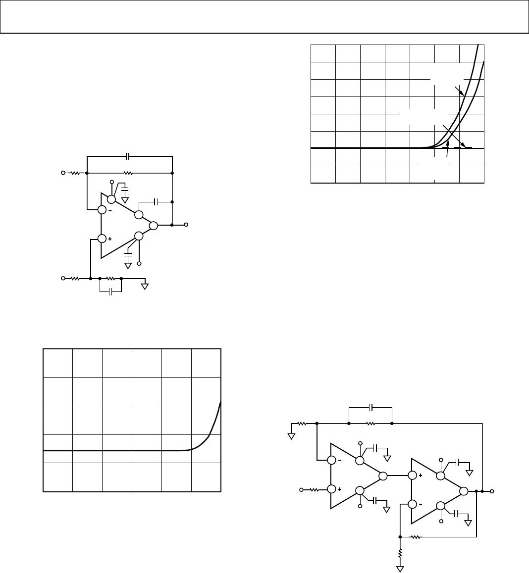
Ultrasound/Sonar Imaging Preamp
The AD600 variable gain amplifier provides the time-controlled
gain (TCG) function necessary for very wide dynamic range
sonar and low frequency ultrasound applications. Under some
circumstances, it is necessary to buffer the input of the AD600
to preserve its low noise performance. To optimize dynamic
range, this buffer should have a maximum of 6 dB of gain. The
combination of low noise and low gain is difficult to achieve.
The input buffer circuit shown in Figure 51 provides 1 nV/√Hz
noise performance at a gain of 2 (dc to 1 MHz) by using 26.1 Ω
resistors in its feedback path. Distortion is only −50 dBc at
1 MHz for a 2 V p-p output level and drops rapidly to better
than −70 dBc at an output level of 200 mV p-p.
*
7
*
*
*
+V
S
V
S
= ±6Vdc
V
OUT
AD797
00846-050
26.1
26.1
6
3
4
2
–V
S
AD600
V
IN
*USE THE POWER SUPPLY BYPASSING SHOWN IN FIGURE 35.
Figure 51. An Ultrasound Preamplifier Circuit
Amorphous (Photodiode) Detector
Large area photodiodes (C
S
≥ 500 pF) and certain image
detectors (amorphous Si) have optimum performance when used
in conjunction with amplifiers with very low voltage (rather than
very low current noise). Figure 52 shows the AD797 used with
an amorphous Si (C
S
= 1000 pF) detector. The response is adjusted
for flatness using capacitor C
L
, and the noise is dominated by
voltage noise amplified by the ac noise gain. The AD797s excellent
input noise performance gives 27 μV rms total noise in a 1 MHz
bandwidth, as shown by Figure 53.
*
7
*
+V
S
I
S
AD797
00846-051
10k
100
C
L
50pF
C
S
1000pF
6
3
4
2
–V
S
V
OUT
*USE THE POWER SUPPLY BYPASSING SHOWN IN FIGURE 35.
Figure 52. Amorphous Detector Preamp
00846-052
100M1k100
100
0
60
20
40
80
10M1M100k10k
FREQUENCY (Hz)
VOLTAGE NOISE (mV rms (0.1Hz FREQUENCY))
V
OUT
(dB Re 1V/µA)
–80
30
–50
–70
–60
–40
NOISE
V
OUT
Figure 53. Total Integrated Voltage Noise and V
OUT
of Amorphous Detector Preamp
Professional Audio Signal Processing—DAC Buffers
The low noise and low distortion of the AD797 make it an ideal
choice for professional audio signal processing. An ideal I-to-V
converter for a current output DAC would simply be a resistor
to ground, were it not for the fact that most DACs do not operate
linearly with voltage on their output. Standard practice is to
operate an op amp as an I-to-V converter, creating a virtual
ground at its inverting input. Normally, clock energy and current
steps must be absorbed by the op amp output stage. However, in
the configuration shown in Figure 54, Capacitor C
F
shunts high
frequency energy to ground while correctly reproducing the
desired output with extremely low THD and IMD.
7
*
*
+V
S
–V
S
AD797
00846-053
C
F
82pF
6
2
C1
2000pF
4
100
3k
AD1862
DAC
3
V
OUT
*USE THE POWER SUPPLY BYPASSING SHOWN IN FIGURE 35.
Figure 54. A Professional Audio DAC Buffer
V
OUT
7
+
V
S
–V
S
AD797
6
2
4
3
1
5
V
OS
ADJUST
00846-054
–IN
+IN
20k
Figure 55. Offset Null Configuration

AD797ARZ-REEL7

Mfr. #:
Manufacturer:
Description:
Microphone Preamplifiers Ultralow Distortion Ultralow Noise
Lifecycle:
New from this manufacturer.
Delivery:
DHL FedEx Ups TNT EMS
Payment:
T/T Paypal Visa MoneyGram Western Union