BGM1013 All information provided in this document is subject to legal disclaimers. © NXP B.V. 2011. All rights reserved.
Product data sheet Rev. 5 — 19 September 2011 3 of 15
NXP Semiconductors
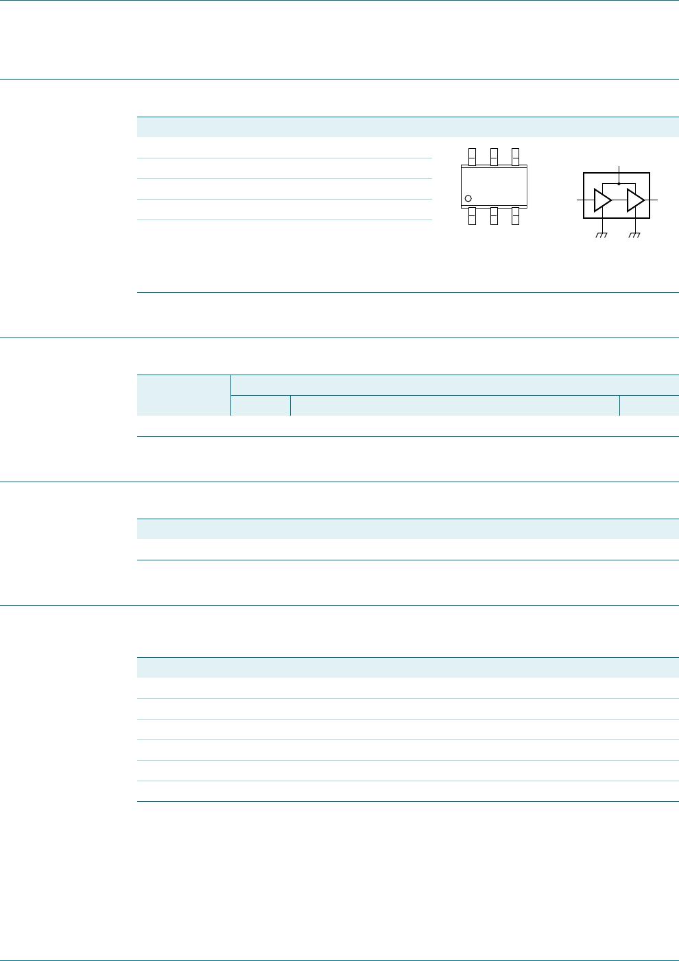
BGM1013
MMIC wideband amplifier)
6. Recommended operating conditions
7. Thermal characteristics
8. Characteristics
Table 6. Operating conditions
Symbol Parameter Conditions Min Typ Max Unit
V
S
supply voltage 4.5 5.0 5.5 V
T
amb
ambient temperature 40 25 85 C
Table 7. Thermal characteristics
Symbol Parameter Conditions Typ Unit
R
th(j-sp)
thermal resistance from junction to solder point P
tot
=200mW; T
sp
90 C 300 K/W
Table 8. Characteristics
V
S
=5 V; I
S
= 27.5 mA; T
j
=25
C; measured on demo board; unless otherwise specified.
Symbol Parameter Conditions Min Typ Max Unit
V
S
DC supply voltage RF input; AC coupled - 5 6 V
I
S
DC supply current 23 27.5 33 mA
s
21
2
insertion power gain f = 100 MHz 34.5 35.2 35.9 dB
f = 1 GHz 34.5 35.5 36.2 dB
f = 1.8 GHz 33.0 34.0 35.2 dB
f = 2.2 GHz 30.5 31.8 33.1 dB
f = 2.6 GHz 25.2 29.7 31.2 dB
f = 3 GHz 24.0 26.1 27.9 dB
s
11
2
input return loss f = 1 GHz 10.1 10.6 - dB
f = 2.2 GHz 9.3 10.2 - dB
s
22
2
output return loss Z
L
=50
f=1GHz 18 20 - dB
f = 2.2 GHz 13 16 - dB
Z
L
=75
f=1GHz 15 17 - dB
f = 2.2 GHz 12 15 - dB
s
12
2
isolation f = 1 GHz 40 42 - dB
f = 2.2 GHz 34 36 - dB
NF noise figure f = 1 GHz - 4.6 4.7 dB
f = 2.2 GHz - 4.9 5.1 dB
B bandwidth 3 dB below flat gain at f = 1 GHz - 2.1 - GHz
K stability factor f = 1 GHz 1.2 1.3 -
f=2.2GHz 0.9 1.0 -
P
L(sat)
saturated load power f = 1 GHz 13.0 14.0 - dBm
f = 2.2 GHz 9.0 10.2 - dBm