BGM1013 All information provided in this document is subject to legal disclaimers. © NXP B.V. 2011. All rights reserved.
Product data sheet Rev. 5 — 19 September 2011 4 of 15
NXP Semiconductors
BGM1013
MMIC wideband amplifier)
9. Application information
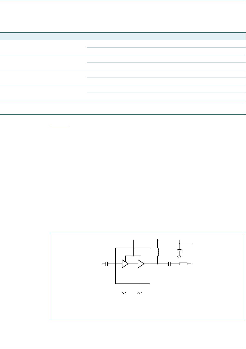
Figure 1 shows a typical application circuit for the BGM1013 MMIC. The device is
internally matched to 50 and therefore does not need any external matching. Output
impedance is also very good to 75 load. The value of the input and output DC blocking
capacitors C1 and C2 should be not more than 100 pF for applications above 100 MHz.
Their values can be used to fine-tune the input and output impedance.
For the RF-choke, optimal results are obtained with a good quality chip inductor like the
TDK MLG1608 (0603) or a wire-wound SMD. The value of the inductor can be used to
fine-tune the output impedance.
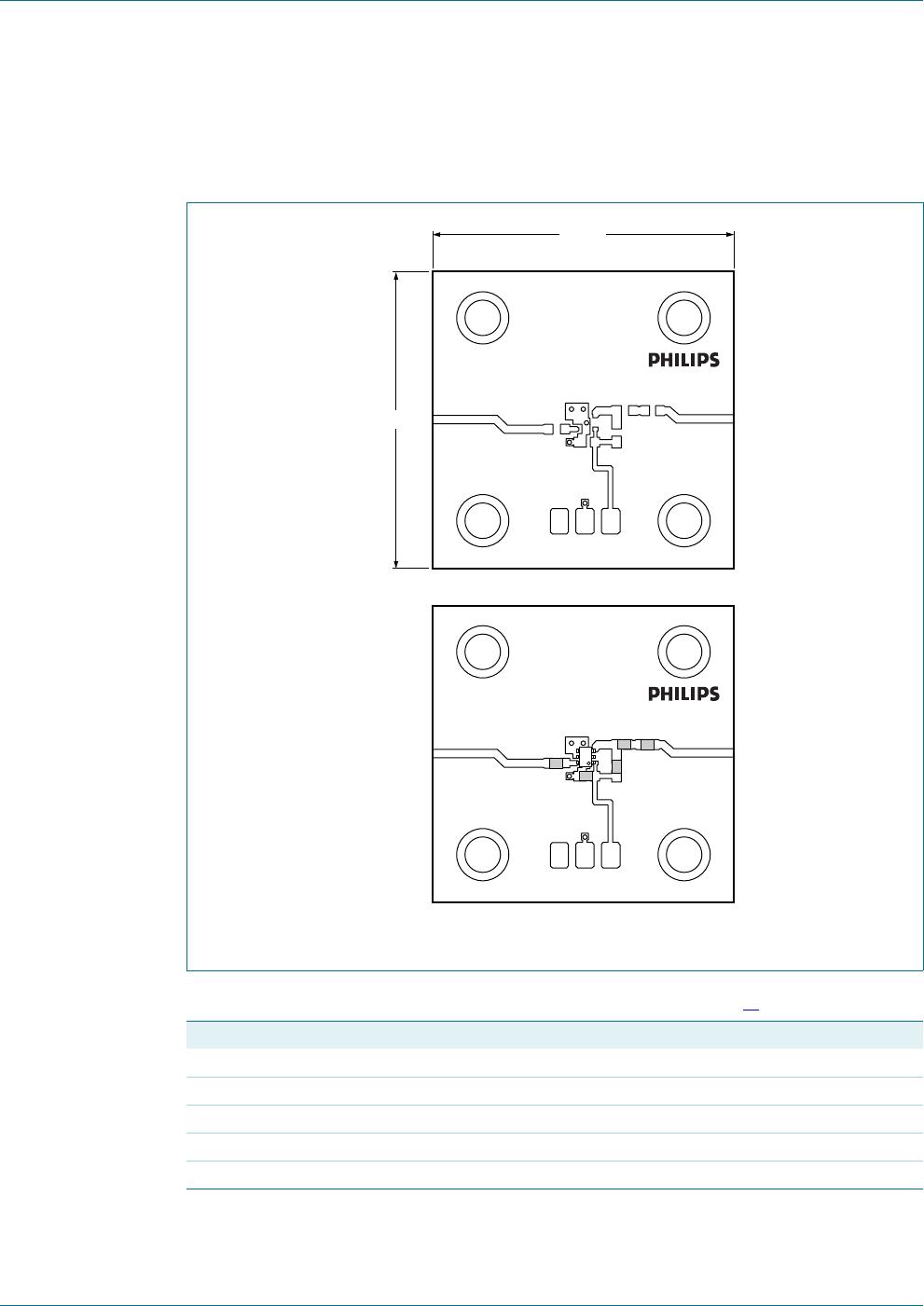
The RF choke and supply decoupling components should be located as close as possible
to the MMIC.
Ground paths must be as short as possible. The printed-circuit board (PCB) top ground
plane must be as close as possible to the MMIC, and ideally directly beneath it. When
using vias, use at least 3 vias for the top ground plane in order to limit ground path
inductance. Supply decoupling with C3 should be from pin 1 to the same top ground
plane.
P
L(1dB)
load power at 1 dB gain
compression
f = 1 GHz 12.0 13.0 - dBm
f=2.2GHz 7.0 8.1 - dBm
IP3
in
input third order intercept point f = 1 GHz 14 12.8 - dBm
f=2.2GHz 15 13.2 - dBm
IP3
out
output third order intercept point f = 1 GHz 21 22.7 - dBm
f = 2.2 GHz 17 18.6 - dBm
IM2 second order intermodulation
product
f
0
= 1 GHz; P
D
= 45 dBm (P
L
= 10 dBm) - 45 43 dBc
f
0
= 1 GHz; P
D
= 40 dBm (P
L
= 5 dBm) - 43 41 dBc
Table 8. Characteristics
…continued
V
S
=5 V; I
S
= 27.5 mA; T
j
=25
C; measured on demo board; unless otherwise specified.
Symbol Parameter Conditions Min Typ Max Unit
(1) R1 is omitted in typical application.
Fig 1. Typical application circuit
001aab389
4 2, 5
BGM1013
SOT363
36
1
GND2GND1
V
S
RF in
V
S
RF out
IN
OUT
L1
C3
C2
C1
R1
(1)