www.vishay.com
4
Document Number: 70818
S11-0975-Rev. D, 16-May-11
Vishay Siliconix
Si9136
This document is subject to change without notice.
THE PRODUCTS DESCRIBED HEREIN AND THIS DOCUMENT ARE SUBJECT TO SPECIFIC DISCLAIMERS, SET FORTH AT www.vishay.com/doc?91000
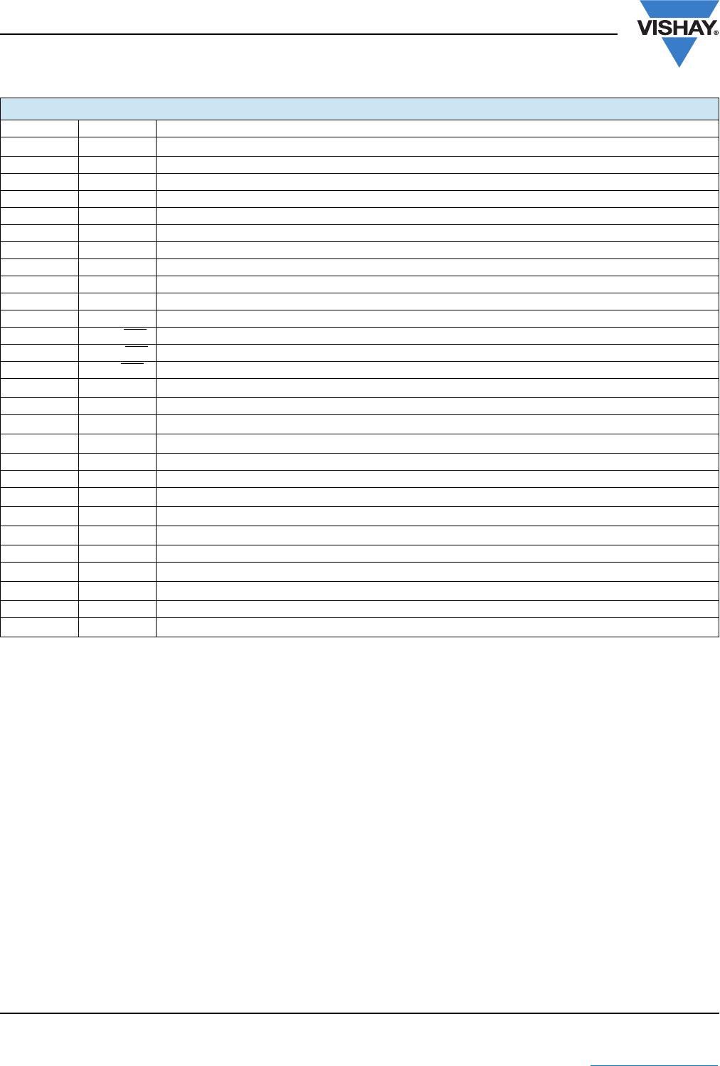
PIN DESCRIPTION
Pin Number Symbol Description
1
CS
3
Current sense input for 3.3 V buck.
2 FBFY Feedback for flyback.
3 BSTFY Boost capacitor connection for flyback converter.
4 DHFY Gate-drive output for flyback high-side MOSFET.
5 LXFY Inductor connection for flyback converter.
6 DLFY Gate-drive output for flyback low-side MOSFET.
7 CSP Current sense positive input for flyback converter.
8 CSN Current sense negative input for flyback converter.
9 GND Analog ground.
10 COMP Flyback compensation connection, if required.
11 REF 3.3 V internal reference.
12 12 ON/OFF
ON and OFF control input for 12 V flyback controller.
13 3.3 ON/OFF
ON and OFF control input for 3.3 V buck controller.
14 5 ON/OFF
ON and OFF control input for 5 V buck controller.
15
CS
5
Current sense input for 5 V buck controller.
16 DH5 Inductor connection for buck 5 V.
17
LX
5
Gate-drive output for 5 V buck high-side MOSFET.
18
BST
5
Boost capacitor connection for 5 V buck converter.
19 DL5 Gate-drive output for 5 V buck low-side MOSFET.
20 PGND Power ground.
21
FB
5
Feedback for 5 V buck.
22
V
L
5 V logic supply voltage for internal circuitry.
23
V
IN
Input voltage
24 DL3 Gate-drive output for 3.3 V buck low-side MOSFET.
25
BST
3
Boost capacitor connection for 3.3 V buck converter.
26
LX
3
Inductor connection for 3.3 V buck low-side MOSFET.
27 DH3 Gate-drive output for 3.3 V buck high-side MOSFET.
28
FB
3
Feedback for 3.3 V buck.

