Expand menu
Hello, Sign in
My Account
0
Cart
Home
Products
Sensors
Semiconductors
Passive Components
Connectors
Power
Electromechanical
Optoelectronics
Circuit Protection
Integrated Circuits - ICs
Main Products
Manufacturers
Blog
Services
About OMO
About Us
Contact Us
Check Stock
SI9136LG-E3
P1-P3
P4-P6
P7-P9
P10-P12
P13-P15
P16-P16
Document Number: 70818
S11-0975-Rev. D, 16-May-11
www.vishay.com
7
Vishay Siliconix
Si9136
This documen
t is subjec
t to change
without notic
e.
THE PRODUCTS DESCRIBED HEREIN AND THIS DOCUMENT AR
E SUBJECT TO SPECIFIC DISCLAIMERS, SET FORTH A
T
www
.vishay
.com/do
c?91000
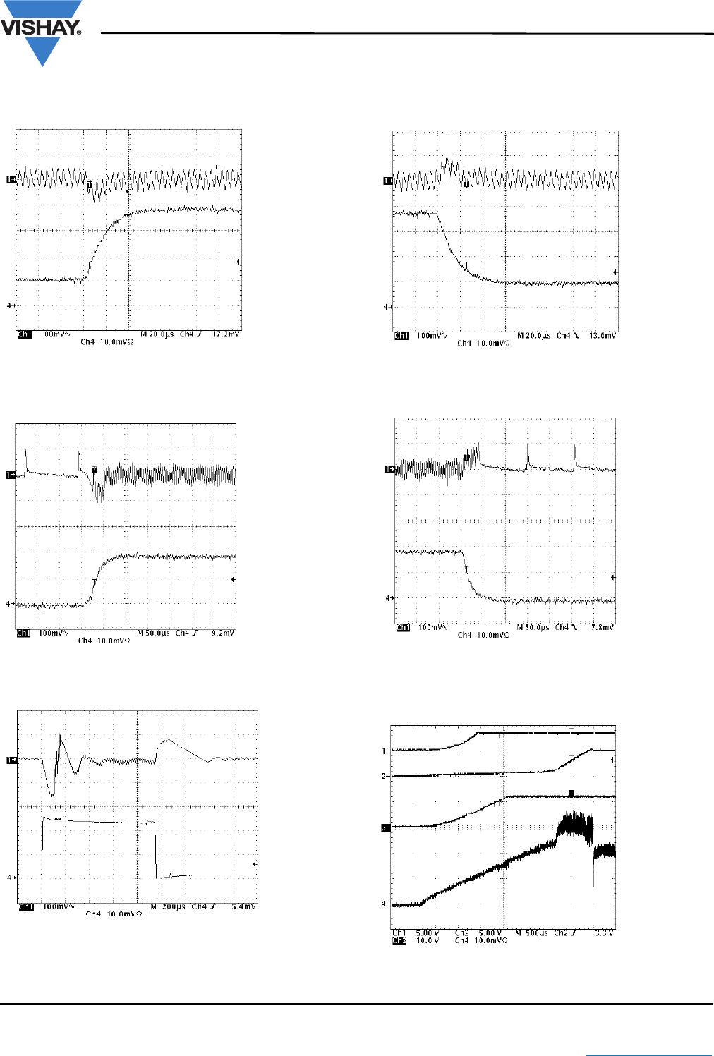
TYPICAL WAVEFORMS
3 V Converter (V
IN
= 10 V)
3 V Converter (V
IN
= 10 V)
12 V Converter (V
IN
= 10 V)
PWM, Loading
Ch1: V
OUT
Ch2: Load
Current (1
A/div)
PSM Õ
PWM
V
OUT
Ch2: Load
Current (1
A/div)
Ch1:
250 mA Transient
Ch1: V
OUT
Ch4: Load
Current
(100 mA/div)
3 V Converter (V
IN
= 10 V)
3 V Converter (V
IN
= 10 V)
Start-Up
PWM, Unloading
Ch1: V
OUT
Ch2: Load
Current (1
A/div)
PWM Õ
PSM
Ch1:
V
OUT
Ch2: Load
Current (1
A/div)
3.3 V
Output
5 V Output
12 V Output
Inductor Current,
5 V Converter
(2 A/div)
www.vishay.com
8
Document Number: 70818
S11-0975-Rev. D, 16-May-11
Vishay Siliconix
Si9136
This docu
ment is subje
ct to change
without noti
ce.
THE PRODUCTS DESCRIBED HEREIN
AND THIS DOCUMENT AR
E SUBJECT TO SPECIFIC DISCLAIMERS, SET FOR
T
H A
T
www
.visha
y
.com/doc?91000
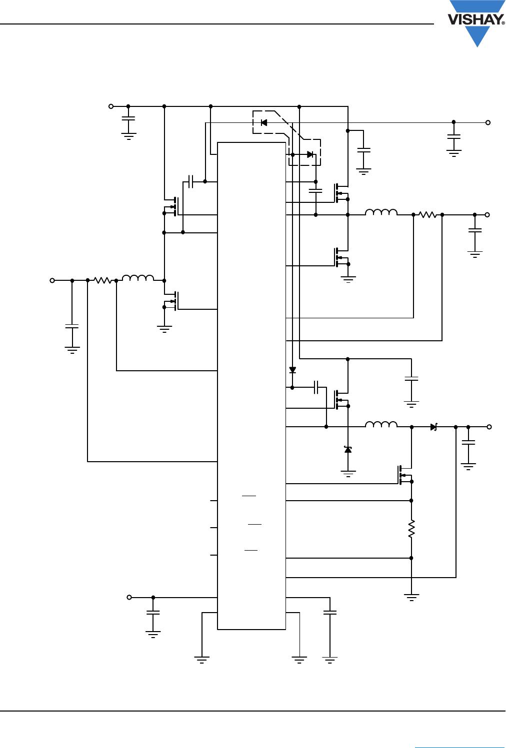
STANDARD APPLICATION CIRCUIT
Figure 1.
BSTFY
DHFY
LXFY
DLFY
CSP
CSN
FBFY
DL5
LX
5
DH5
BST
5
V
L
COMP
PGND
FB
5
CS
5
V
IN
BST
3
DH3
LX
3
DL3
CS
3
FB3
5 ON/OFF
REF
GND
3.3 ON/OFF
12 ON/OFF
V
IN
C7
33 µ
F
C1
0.1 µ
F
Q1
Si4416DY
C6
330 µ
F
+ 3.3 V
L2
10 µ
H
Q3
Si4812DY
R
1
R
cs2
0.02
Ω
C1
1
1 µ
F
+ 3.3 V up
to 1 mA
CMPD2836
D1
D2
CMPD2836
C2
0.1 µ
F
D3
CMPD2836
C8
0.1 µ
F
Q2
Si4416DY
Q4
Si4812DY
C4
33 µ
F
D5, D1FS4
Q5
Si2304DS
L3, 10 µ
H
Q6
Si2304DS
R
6
R
cs3
C10
100 µ
F
C9
4.7 µ
F
D4, D1FS4
+ 12 V 0 to
250 mA
L1, 10 µ
H
R
7
R
cs1
0.02
Ω
C5
4.7 µ
F
+ 5 V up to 30 mA
C3
330 µ
F
+ 5 V
C12
120 pF
Document Number: 70818
S11-0975-Rev. D, 16-May-11
www.vishay.com
9
Vishay Siliconix
Si9136
This documen
t is subjec
t to change
without notic
e.
THE PRODUCTS DESCRIBED HEREIN AND THIS DOCUMENT AR
E SUBJECT TO SPECIFIC DISCLAIMERS, SET FORTH A
T
www
.vishay
.com/do
c?91000
TIMING DIAGRAMS
Figure 2. Converter is Enable
d Before V
IN
is Applied
ON/OFF
V
IN
V
L
V
REF
OSC EN
(Sysmon EN)
OSC
f
max
(SS)
DH
D
L
The converter is enabled
V
IN
is applied
LDO is activated
after V
IN
is applied
REF circuit is activated
after V
L
becomes
available
After V
REF
goes above
2.4 V
, the converter is
turned on
Oscillator is activated
Slow soft-start gradually
increases the maximum
inductor current
High-side gate drive duty
ratio gradually increases
to maximum
Low-side gate drive
4 ms
2.4 V
t
BBM
Figure 3. Converter is Enabled After V
IN
is Applied
ON/OFF
V
IN
V
L
V
REF
OSC EN
(Sysmon EN)
OSC
f
max
(SS)
DH
DL
The converter is
enabled
V
IN
is applied
LDO is activated
after V
IN
is applied
REF circuit is activated
after V
L
becomes
available
After V
REF
goes above
2.4 V
, the converter is
turned on
Oscillator is activated
Slow soft-start gradually
increases the maximum
inductor current
2.4 V
4 ms
P1-P3
P4-P6
P7-P9
P10-P12
P13-P15
P16-P16
SI9136LG-E3
Mfr. #:
Buy SI9136LG-E3
Manufacturer:
Vishay / Siliconix
Description:
Switching Controllers Multi-Out Pwr-Supply Controller
Lifecycle:
New from this manufacturer.
Delivery:
DHL
FedEx
Ups
TNT
EMS
Payment:
T/T
Paypal
Visa
MoneyGram
Western
Union
Products related to this Datasheet
SI9136LG-E3