PowerPAK
®
SO-8 Mounting and Thermal Considerations
APPLICATION NOTE
Application Note AN821
www.vishay.com
Vishay Siliconix
Revision: 16-Mai-13
3
Document Number: 71622
For technical questions, contact: powermosfettechsupport@vishay.com
THIS DOCUMENT IS SUBJECT TO CHANGE WITHOUT NOTICE. THE PRODUCTS DESCRIBED HEREIN AND THIS DOCUMENT
ARE SUBJECT TO SPECIFIC DISCLAIMERS, SET FORTH AT www.vishay.com/doc?91000
THERMAL PERFORMANCE
Introduction
A basic measure of a device’s thermal performance
is the junction-to-case thermal resistance, R
thJC
, or the
junction-to-foot thermal resistance, R
thJF
This parameter is
measured for the device mounted to an infinite heat sink and
is therefore a characterization of the device only, in other
words, independent of the properties of the object to which
the device is mounted. Table 1 shows a comparison of
the DPAK, PowerPAK SO-8, and standard SO-8. The
PowerPAK has thermal performance equivalent to the
DPAK, while having an order of magnitude better thermal
performance over the SO-8.
Thermal Performance on Standard SO-8 Pad Pattern
Because of the common footprint, a PowerPAK SO-8
can be mounted on an existing standard SO-8 pad pattern.
The question then arises as to the thermal performance
of the PowerPAK device under these conditions. A
characterization was made comparing a standard SO-8 and
a PowerPAK device on a board with a trough cut out
underneath the PowerPAK drain pad. This configuration
restricted the heat flow to the SO-8 land pads. The results
are shown in figure 5.
Fig. 5 PowerPAK SO-8 and Standard SO-0 Land Pad Thermal
Path
Because of the presence of the trough, this result suggests
a minimum performance improvement of 10 °C/W by using
a PowerPAK SO-8 in a standard SO-8 PC board mount.
The only concern when mounting a PowerPAK on a
standard SO-8 pad pattern is that there should be no traces
running between the body of the MOSFET. Where the
standard SO-8 body is spaced away from the pc board,
allowing traces to run underneath, the PowerPAK sits
directly on the pc board.
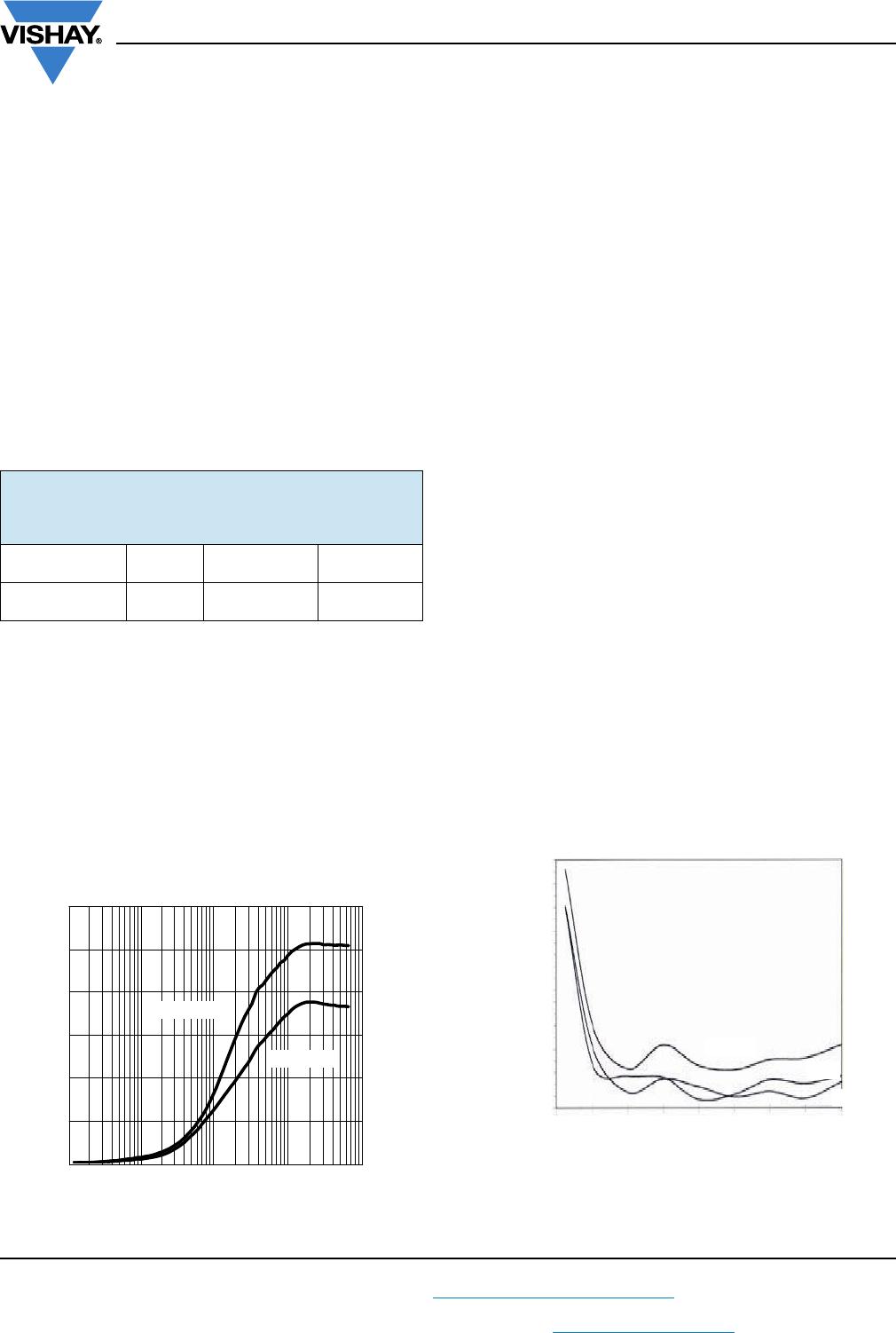
Thermal Performance - Spreading Copper
Designers may add additional copper, spreading copper, to
the drain pad to aid in conducting heat from a device. It is
helpful to have some information about the thermal
performance for a given area of spreading copper.
Figure 6 shows the thermal resistance of a PowerPAK SO-8
device mounted on a 2-in. 2-in., four-layer FR-4 PC board.
The two internal layers and the backside layer are solid
copper. The internal layers were chosen as solid copper to
model the large power and ground planes common in many
applications. The top layer was cut back to a smaller area
and at each step junction-to-ambient thermal resistance
measurements were taken. The results indicate that an area
above 0.3 to 0.4 square inches of spreading copper gives no
additional thermal performance improvement. A
subsequent experiment was run where the copper on the
back-side was reduced, first to 50 % in stripes to mimic
circuit traces, and then totally removed. No significant effect
was observed.
Fig. 6 Spreading Copper Junction-to-Ambient Performance
TABLE 1 - DPAK AND POWERPAK SO-8
EQUIVALENT STEADY STATE
PERFORMANCE
DPAK
PowerPAK
SO-8
Standard
SO-8
Thermal
Resistance R
thJC
1.2 °C/W 1 °C/W 16 °C/W
Si4874DY vs. Si7446DP PPAK on a 4-Layer Board
SO-8 Pattern, Trough Under Drain
Pulse Duration (sec)
)
s
ttaw/
C
( e
cn
adep
m
I
0.0001
0
1
50
60
10
100000.01
40
20
Si4874DY
Si7446DP
100
30
PowerPAK
®
SO-8 Mounting and Thermal Considerations
APPLICATION NOTE
Application Note AN821
www.vishay.com
Vishay Siliconix
Revision: 16-Mai-13
4
Document Number: 71622
For technical questions, contact: powermosfettechsupport@vishay.com
THIS DOCUMENT IS SUBJECT TO CHANGE WITHOUT NOTICE. THE PRODUCTS DESCRIBED HEREIN AND THIS DOCUMENT
ARE SUBJECT TO SPECIFIC DISCLAIMERS, SET FORTH AT www.vishay.com/doc?91000
SYSTEM AND ELECTRICAL IMPACT OF
PowerPAK SO-8
In any design, one must take into account the change in
MOSFET R
DS(on)
with temperature (figure 7).
Fig. 7 MOSFET R
DS(on)
vs. Temperature
A MOSFET generates internal heat due to the current
passing through the channel. This self-heating raises the
junction temperature of the device above that of the PC
board to which it is mounted, causing increased power
dissipation in the device. A major source of this problem lies
in the large values of the junction-to-foot thermal resistance
of the SO-8 package.
PowerPAK SO-8 minimizes the junction-to-board thermal
resistance to where the MOSFET die temperature is very
close to the temperature of the PC board. Consider two
devices mounted on a PC board heated to 105 °C by other
components on the board (figure 8).
Fig. 8 Temperature of Devices on a PC Board
Suppose each device is dissipating 2.7 W. Using the
junction-to-foot thermal resistance characteristics of the
PowerPAK SO-8 and the standard SO-8, the die
temperature is determined to be 107 °C for the PowerPAK
(and for DPAK) and 148 °C for the standard SO-8. This is a
2 °C rise above the board temperature for the PowerPAK
and a 43 °C rise for the standard SO-8. Referring to figure 7,
a 2 °C difference has minimal effect on R
DS(on)
whereas a
43 °C difference has a significant effect on R
DS(on)
.
Minimizing the thermal rise above the board temperature by
using PowerPAK has not only eased the thermal design but
it has allowed the device to run cooler, keep r
DS(on)
low, and
permits the device to handle more current than the same
MOSFET die in the standard SO-8 package.
CONCLUSIONS
PowerPAK SO-8 has been shown to have the same thermal
performance as the DPAK package while having the same
footprint as the standard SO-8 package. The PowerPAK
SO-8 can hold larger die approximately equal in size to the
maximum that the DPAK can accommodate implying no
sacrifice in performance because of package limitations.
Recommended PowerPAK SO-8 land patterns are provided
to aid in PC board layout for designs using this new
package.
Thermal considerations have indicated that significant
advantages can be gained by using PowerPAK SO-8
devices in designs where the PC board was laid out for
the standard SO-8. Applications experimental data gave
thermal performance data showing minimum and
typical thermal performance in a SO-8 environment, plus
information on the optimum thermal performance
obtainable including spreading copper. This further
emphasized the DPAK equivalency.
PowerPAK SO-8 therefore has the desired small size
characteristics of the SO-8 combined with the attractive
thermal characteristics of the DPAK package.
0.6
0.8
1.0
1.2
1.4
1.6
1.8
-50 -25 0 25 50 75 100 125 150
V
GS
= 10 V
I
D
= 23 A
On-Resistance vs. Junction Temperature
T
J
- Junction Temperature (°C)
)dezilamroN(( ecnatsiseR-nO -R
)no(SD
)
0.8 °C/W
107 °C
PowerPAK SO-8
16 C/W
148 °C
Standard SO-8
PC Board at 105 °C
Application Note 826
Vishay Siliconix
Document Number: 72599 www.vishay.com
Revision: 21-Jan-08 15
APPLICATION NOTE
RECOMMENDED MINIMUM PADS FOR PowerPAK
®
SO-8 Single
0.174
(4.42)
Recommended Minimum Pads
Dimensions in Inches/(mm)
0.260
(6.61)
0.024
(0.61)
0.154
(3.91)
0.150
(3.81)
0.050
(1.27)
0.050
(1.27)
0.032
(0.82)
0.040
(1.02)
0.026
(0.66)
Return to Index
Return to Index

SI7848BDP-T1-GE3

Mfr. #:
Manufacturer:
Vishay / Siliconix
Description:
MOSFET 40V Vds 20V Vgs PowerPAK SO-8
Lifecycle:
New from this manufacturer.
Delivery:
DHL FedEx Ups TNT EMS
Payment:
T/T Paypal Visa MoneyGram Western Union

Products related to this Datasheet